
Conventional switches (such as MOSFETs or IGBTs) usually have a forward conduction state and a reverse blocking state. For instance, by using the main diode of a MOSFET or adding an anti-parallel diode to an IGBT, the third quadrant can be used for conduction. This allows for reverse conduction of the flow, but there is no gate control. These devices can typically achieve switchable bidirectional streaming by using two of these devices in a back-to-back (B2B) configuration.
Since the effective state resistance (RDSON) is doubled, parallel groups of these devices are required to return to the value obtained using the one-way switch. Single-chip devices capable of performing such fourth-quarter operations can reduce system size and complexity by replacing four active switches with a single device. The use of GAN in BDS can create further advantages in certain applications due to its lower loss and the ability to switch faster than traditional Si-based devices.
Let's take a look at some key applications where BDS devices can play a crucial role:
AC switch: In many applications, the concept of bidirectional AC-AC power flow is very attractive. Consider a solar micro-inverter. The standard approach is to create an intermediate DC link voltage and then convert it to an AC voltage, which can be fed to the grid or used by consumers. Dc link capacitors can be large, increasing their size and cost. The AC-DC-AC process involves the reduction of efficiency through each power conversion stage. Another example is the on-board charger (OBC), where a single-stage isolated power conversion can be achieved using an AC switch. About 45 years ago, a matrix switch was first proposed. Two three-phase ports can be connected to the 9 BDS devices at the intersection point, and the voltage, frequency and power factor can be converted. Traditional variable frequency drives (VFDS) typically adopt two-stage conversions including AC-DC and DC links, followed by a DC-AC inverter. When using a diode rectifier, harmonics will be generated, and when braking the motor, the power supply cannot be regenerated. Dc link capacitors are typical failure points and may be bulky. It is estimated that VFDS consume more than 60% of the electricity in industrial applications. Therefore, making these drives more reliable, robust and efficient, while increasing the power density, can have a significant positive impact, and BDS provides a way to achieve this goal. Smaller drivers may be integrated with the motor, thereby gaining further advantages in reducing cables and parasites.
Replacing the B2B switch in a conventional AC-DC converter: Let's consider the example of the Vienna rectifier. This is a simple integrated boost diode bridge with an added BTB device that connects the midpoint of the generated DC back to the AC side. These BTB switches can feed current into the input inductor and compensate for 3rd harmonic distortion, thereby controlling the shape of the input current. This popular rectifier has been used in telecommunication power supplies, fast offline electric vehicle charging, etc. Essentially, a T-type converter is a diode in a Vienna bride that replaces the diode of an active switch such as a MOSFET. These three-stage inverters allow for bidirectional power flow and can be used in many solid-state transformer (SST) applications. The evil inverter has found many uses in photovoltaic (PV) applications. Here, the BDS creates a bypass on the AC power supply, switching at the grid frequency and allowing the reactive current to flow. In these popular converter designs, replacing the current multi-advisor BD with the monolithic gan bds brings the benefit of lower device counts, while using GAN for faster switching can reduce the size of passive components. The BDS devices used in these three-layer topologies only need to maintain half of the total DC voltage.
Current source inverter (CSI) : CSI feed induction motor with stator current. Sinusoidal current entering the motor can significantly improve the motor design and reliability. The large inductors used in CSIS can provide inherent overload and short-circuit protection. The CSI requires a switch to block the voltage in both directions, so MOSFETs or IGBTs need to be connected in series with diodes. When using WBG equipment, the voltage source inverter (VSI) is not very tolerant of using fast switching because the instantaneous overvoltage in the switching waveform increases the EMI risk. This will emphasize the motor windings and bearings. Although CSI inverters face unique challenges, such as higher costs due to increased control complexity, they may be suitable for high-power motor drives, electric aircraft, and HVDC transmission states. The WBG device used in the CSI driver can switch at high frequency, thereby reducing the size of the inductor. As the output capacitor forms a low-pass filter, the EMI risk is reduced. The GAN BDS device 2 has been proved in the CSI design. Although bidirectional voltage blocking is required, the unidirectional current flow meets the requirements, thus it is possible to simplify the required gating. This will be further discussed below.
AC solid-state circuit breaker (SCCB) and battery disconnection: AC SCCB requires bidirectional, reliable overvoltage characteristics, low state resistance, fast response time, low thermal resistance packaging, and high current fault clearance to? Within the range of S In this application, the device usually operates under static conditions. Replacing with a single GAN BDS MOSFET or IGBT mechanical circuit breaker or anti-series combination has advantages in lower molds and more efficient equipment. One significant advantage in the use of Gan Hemt is the absence of a significant Spirito effect, which, under certain conditions, can reduce the safe operating area (SOA) of Si-based devices. Battery disconnection switches, such as in the charging circuits of mobile phones and laptops. They provide disconnection under overvoltage conditions, thereby offering important protection functions. The BDS in these applications, for very low state resistances (<10MΩ), typically employs a combined source, single-connection method, rather than the combined drainage, two-gate method used in the aforementioned other applications. This combined drainage BDS device will now be described in more detail.
gan hv-bds
At the recent Infineon 2025 Wide-Bandgap Developer Forum, Dr. Kennith Leong, the principal of Coolgan HV BDS and a product definition and concept engineer, described Infineon's GAN BDS Switch in detail. The rated values of the HV BDS switch are 650 V and 850 V, and it is based on Infineon's gate Injection Transistor (GIT) GAN technology. The merged central drainage area connects the two gates and sources in these HV BDS devices. Infineon also plans to release the MV BDS switch, which has a rated function of 40 V - 120 V and is used for static battery disconnection applications. These applications adopt Schottky Gate Gan Hemt Technology and are designed with two inserters, single gates and common sources.
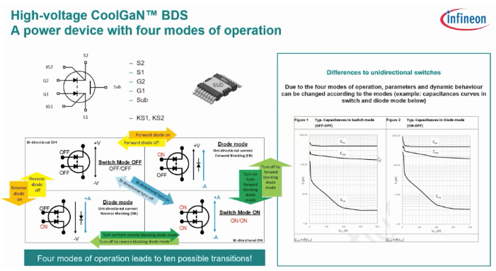
Figure 1 shows the four operation modes of the HV BDS device. When both doors are open, the device shows bidirectional conduction through the origin of the VDS-IDS parameter space. When only one door is open, the diode mode of the equipment will be displayed to effectively control the rotation when the source supply potential (VSD) of the off-door equipment exceeds the effective threshold voltage (VTH-VGS) of HEMT. In GIT devices, this occurs when <2V. When both doors are closed, the blockage of the equipment under voltage is significantly greater than that of the rated equipment.
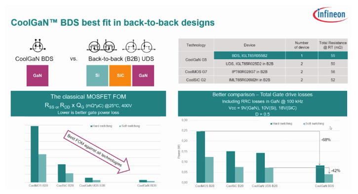
The comparison of power losses under hardening and soft switching is shown in Figure 2. The B2B SI and SIC MOSFETs here are compared with GAN BDS, so the net RDSON is the same. As can be seen, at a switching frequency of 100 kHz, BDS can observe a significant improvement in losses. Shared drainage outlets can significantly improve specific RDSON, thereby allowing for a lower clear mold layer area and reducing switching and dynamic conduction losses. An important improvement observed in these BDS devices is the self-limiting short-circuit behavior, which enables the device to pass through repeated 10-100? s test shows a significant improvement in the unidirectional gan hemts of this feature.
免责声明: 本文章转自其它平台,并不代表本站观点及立场。若有侵权或异议,请联系我们删除。谢谢! Disclaimer: This article is reproduced from other platforms and does not represent the views or positions of this website. If there is any infringement or objection, please contact us to delete it. thank you! |

WeChat Official Account

WeChat Service
 Email
Email QQ
QQ 13823761625
