
Physical structure
Compared with the traditional gallium nitride devices based on sapphire wafers, silicon-based gallium nitride devices significantly reduce the manufacturing cost of the devices, which paves the way for the large-scale application of gallium nitride power semiconductor devices. Figure 1 shows the typical physical structure of a GaN transistor, where a highly conductive two-dimensional electron gas (2DEG) channel with high mobility is formed at the boundary between the AlGaN layer and the GaN layer. Compared with silicon transistors that rely on minority carriers (loosely bound in the silicon lattice) for conduction, the 2DEG channels in GaN transistors exhibit higher electron density and electron mobility, making them suitable for high-current and high-power applications. According to the differences in gate structure and material as well as the turn-on threshold voltage caused by gate doping, the existing GaN transistors mainly fall into two categories: depletion-type GaN transistors and enhance-type GaN transistors.
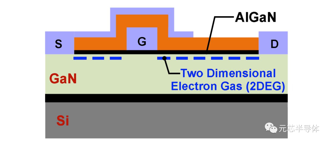
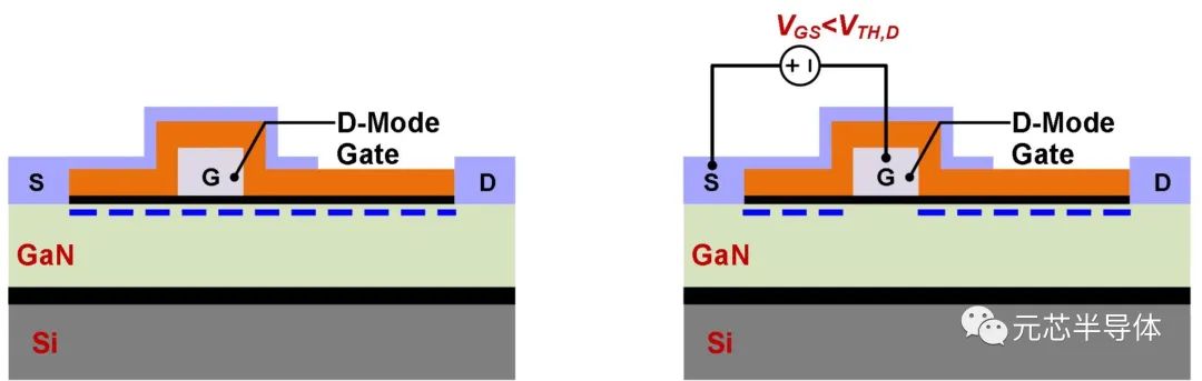
Figure 2 shows the depletion-mode GaN transistor (a) in the normally open state and (b) in the off state
The working characteristics of GaN devices
To clarify the working principle of the enhanced GaN transistor, Figure 4 shows the transport characteristic curve. After VGS reaches nearly 1.7V, the transistor begins to conduct. Due to the high electron mobility of GaN materials, GaN transistors exhibit high transconductance gain and large current conduction capability. For example, at a VGS of 3V, a typical GaN transistor can conduct a saturation current IDS of 5A. In addition, the saturation current of GaN power transistors shows a negative temperature coefficient as the temperature increases, which can protect power devices from permanent damage under high-temperature and high-power operation conditions.
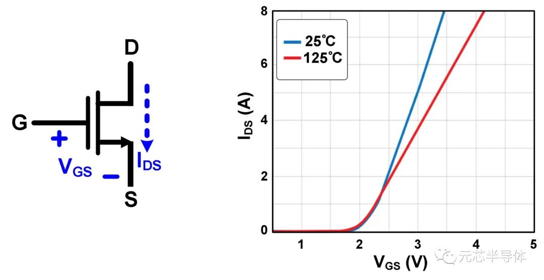
Figure 4 Transmission characteristics of the enhanced GaN transistor
To compare the gate capacitances of GaN transistors and silicon transistors, several typical devices were selected and their gate charge QG parameters were compared, as shown in Table 1. Compared with traditional silicon devices, GaN devices have a wide bandgap voltage and high electron mobility. Under a withstand voltage of 100V and the same on-resistance RDS(ON), the gate charge of GaN transistors is 12 times smaller than that of silicon devices, making GaN devices ideal switching power devices in high-frequency and high-efficiency switching power supply systems.
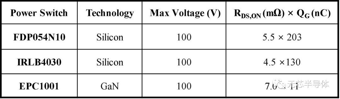
Table 1 Comparison of gate charge QG between silicon and GaN devices
Figure 5 shows the on-resistance RDS(ON) at different gate driving voltages VGS. When VGS approaches the maximum gate voltage, RDS(ON) is the lowest, and the device channel has high conductivity. Therefore, in order to reduce the conduction loss of GaN devices, it is necessary to maximize the gate drive voltage of GaN transistors without damaging the gate structure. In the application of high-current systems where GaN transistors are connected in parallel, due to the positive temperature coefficient of the GaN transistor RDS(ON), it has similar characteristics to silicon transistors and is easy to be connected in parallel to expand the power range.
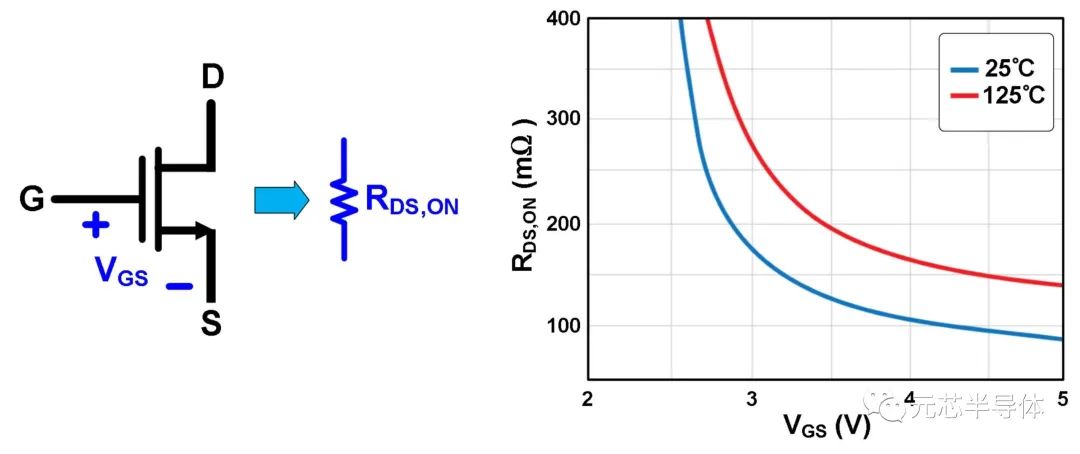
Figure 5. On-resistance at different VGS gate voltages
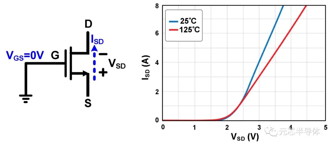
Figure 6. Reverse conduction of enhanced GaN transistors
As shown in Figure 6, when the gate voltage of the GaN is zero, the electrons in the channel are completely exhausted, which forces the GaN transistor to be in the off state. However, as the drain voltage further decreases, a positive bias will be generated between the gate and the drain, attracting electrons beneath the gate to form a conductive channel. Due to the asymmetric structure of the drain and source of GaN transistors, reverse conduction presents a high resistance value. For example, if a current of 4A is to be conducted in reverse, the drain voltage becomes -3V (VSD=3V). In addition, since there are no minority carriers involved in conduction, GaN transistors have no reverse recovery loss, which significantly reduces switching losses and makes them highly suitable for high-frequency switching applications.
免责声明: 本文章转自其它平台,并不代表本站观点及立场。若有侵权或异议,请联系我们删除。谢谢! Disclaimer: This article is reproduced from other platforms and does not represent the views or positions of this website. If there is any infringement or objection, please contact us to delete it. thank you! |

WeChat Official Account

WeChat Service
 Email
Email QQ
QQ 13823761625
