
Question: Can the output switching noise of the ultra-low noise μModule regulator be further reduced?
Answer: The output noise of the ultra-low noise Module regulator can be reduced by more than 90% by using a second-order output filter. When choosing capacitor and inductor components, caution must be exercised to ensure that the control loop can operate quickly and stably. This design is particularly beneficial for wireless and radio frequency applications because the fast transient response can effectively shorten the system blanking time and improve the signal processing efficiency. The noise level of this method is comparable to that of LDO, and its efficiency is comparable to that of a switching regulator.
The power consumption of noise-sensitive devices is constantly increasing. Applications such as medical ultrasound imaging systems, 5G transceivers, and automatic test equipment (ATE) require achieving high output current (>5 A), low noise levels, and high bandwidth on small PCBS. Due to the high demand for output current, the traditional two-stage (step-down + low dropout (LDO) regulator) solution used previously required a large PCB area, resulting in high power consumption and thus was not very popular.
LTM4702 Ultra-low noise? Does the Module regulator adopt ADI's proprietary Silent Switcher? The technology combines ultra-fast transient response and ultra-low noise characteristics. Thanks to this, the efficiency of this device can be comparable to that of synchronous switching regulators, making it an ideal choice for high-current and noise-sensitive applications. In many applications, this solution can eliminate the LDO circuit, thereby saving approximately 60% of the LDO cost, at least 4 W of LDO power consumption, and 2 cm? The above LDO PCB space (including the gap).
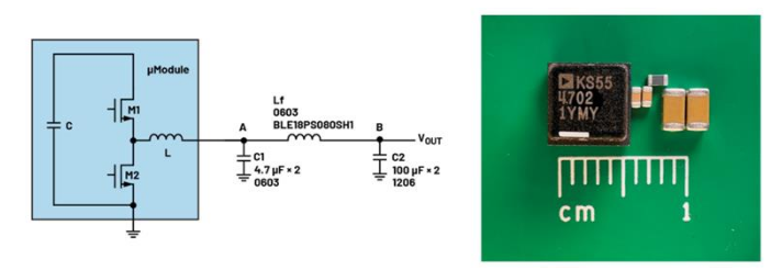
Loop analysis of the second-order LC output filter design In current-mode step-down regulators, the output impedance is the controlled object. Figure 1 shows the circuit of the second-order LC and its typical Bode diagram. In order to accurately adjust the DC voltage even when there is a load, it is necessary to detect the remote node B of VOUT.
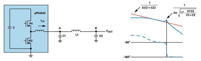
Figure 1. Current-mode step-down regulator and second-order LC and its typical Bode plot
The conversion function from VOUT to iLO is:
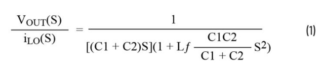
It can be known from the transformation function (Formula 1) that the second-order LC filter will introduce double poles with frequencies of the resonant frequency. It can be seen from the typical Bode plot in Figure 1 that there is a steep 90° phase delay at the resonant frequency. To ensure stability, the resonant frequency should be 4 to 5 times higher than the control loop bandwidth. This is to avoid the 90° phase delay that may cause instability. In addition, to attenuate the switching frequency ripple to a sufficiently low level, this resonant frequency should be set to 1/5 to 1/4 of the switching frequency, so that the LC filter can provide sufficient filtering effect. There exists a trade-off relationship between the attenuation gain at the switching frequency and the control loop bandwidth. However, this method is helpful for selecting the resonant frequency and determining the appropriate LC value.
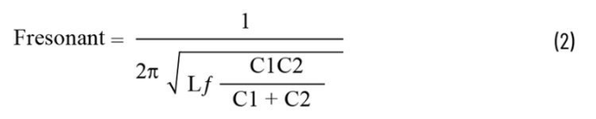
In order to maintain similar load transient performance, the output impedance before and after adding the LC filter should remain consistent. In other words, whether there is an LC filter or not, the output capacitors should be approximately the same. Based on past experience, the capacitance value of C2 in Figure 1 can be similar to that without LC, while C1 can use a much smaller capacitance so that C1 can dominate the resonant frequency position. Since C1 is much smaller than C2, Formula 2 can be simplified to Formula 3:
It is recommended that C1 be at least one-tenth of the value of C2. After selecting C1, the Lf value can be calculated using the resonant frequency in Formula 3. By checking the availability of the actual components, the appropriate C1 and Lf values can be determined.
In the design of an effective second-order LC filter, the selection of capacitive and inductive components is of vital importance. The second-order LC filter needs to provide sufficient attenuation at the switching frequency. The switching frequency of the ultra-low noise Module regulator is relatively high, approximately 1 MHz to 3 MHz. Therefore, the inductors and capacitors in the second-order LC need to have good high-frequency characteristics. The selection requirements for C2 are similar to those for designs without LC, so they are not discussed here. The selection criteria for C1 and Lf are as follows.
Selection criteria for C1 capacitors. The self-resonant frequency of C1 must be higher than the switching frequency. The impedance of C1 at the switching frequency is the key to the second-order LC design. It is recommended to use ceramic capacitors, whose self-resonant frequency can be determined by referring to the relationship curve between their impedance and frequency. Generally, typical ceramic capacitors of 0603 or 0805 size are ideal choices, and their self-resonant frequency must be above 3 MHz. To withstand the required current, the RMS current rating should be high enough. Assuming that all AC ripples pass through C1, then the ceramic capacitor should be able to handle larger RMS ripple currents. The current capacity of ceramic capacitors can be determined by referring to the relationship curve between the temperature rise and the current. Based on experience, for capacitors of size 0603, approximately 4 A rms is a good choice.
For Lf inductors with output currents below 8A, it is recommended to use ferrite beads as they have excellent high-frequency characteristics and a compact size. Ferrite magnetic beads also help to suppress extremely high frequency spikes. For output currents above 8A or when a larger inductance is required, it may be difficult to find suitable ferrite beads. Therefore, it is recommended to use traditional shielded inductors. Select ferrite beads/inductors with A sufficiently large RMS current rating. For example, for output currents below 8 A, choose inductors with an RMS current rating of 8 A. It is recommended that the inductance value of the selected device be less than? 10% of the inductance value of the Module device.
Ultra-low noise? Module Design Example Figure 2 shows the design example of LTM4702. This scheme combines the characteristics of ultra-low electromagnetic interference (EMI) radiation and ultra-low RMS noise, and the switching frequency can be adjusted within the range of 300 kHz to 3 MHz. In the design example, the switching frequency is set to 2 MHz to optimize the noise performance of applications ranging from 12 VIN to 1 VOUT. According to the proposed LC filter design method, the resonant frequency rate of the second-order LC is set at 400 kHz to 500 kHz, which is 1/5 to 1/4 of the switching frequency.
The comparison of noise measurement is shown in Figure 3. At a switching frequency of 2 MHz, the output switching ripple without LC is 234 V, and it is significantly reduced to 15 V after adding 0603 ferrite beads.


Conclusion: How to support high-current applications while minimizing noise and ensuring high efficiency and stability is a thorny problem. Adding a second-order LC filter can significantly reduce noise, but if not optimized properly, it may lead to circuit instability. In order to reduce the noise as much as possible without affecting the stability, an optimized second-order LC filter should be used. Carefully selecting the required inductors and capacitors based on the switching frequency, control loop bandwidth and resonant frequency can effectively reduce switching noise while maintaining fast transient response and high bandwidth characteristics.
免责声明: 本文章转自其它平台,并不代表本站观点及立场。若有侵权或异议,请联系我们删除。谢谢! Disclaimer: This article is reproduced from other platforms and does not represent the views or positions of this website. If there is any infringement or objection, please contact us to delete it. thank you! |

WeChat Official Account

WeChat Service
 Email
Email QQ
QQ 13823761625
