
In the field of power semiconductors, gallium nitride (GaN) is hailed as the "core of next-generation switching devices" due to its high-frequency and high-efficiency characteristics. This technology has now entered thousands of households through fast charging. However, how to continuously leverage the power advantages of gan and achieve the same level of popularity as fast charging heads in various fields has always been an industry challenge.
Texas Instruments (TI) has recently launched the GaN LMG365x in the industry-standard TOLL package to meet customers' demands for multiple suppliers. At the same time, it continues to leverage the characteristics of highly integrated drive protection and power, continuously contributing to the large-scale application of GaN in fields such as data centers, solar micro-inverters, TV power supplies, and even in-vehicle OBC.
From discrete to Integrated: Breaking the "parasitic parameter" Curse of High-Frequency Design
Traditional discrete GaN devices face two major pain points in high-frequency applications: the drive is difficult to do, and the protection circuit is also difficult to do. TI's LMG365x series devices, through the design concept of "package as system", deeply integrate the gate driver, protection circuit and power transistor. This is also the product strategy adopted by TI since it launched its first commercial GaN power device.
You Shengyang, the system manager of Texas Instruments, stated that the switching frequency of gallium nitride is relatively fast. Therefore, if a discrete solution is adopted, the parasitic inductance between the driver and the FET is relatively high, which will limit the operating frequency. This limits the significance of using GaN and prevents it from achieving its maximum value. And through integration, more frequent operations can be achieved.
At the same time, due to the extremely fast switching speed of GaN, it will bring higher EMI interference, which requires more attention in PCB layout. If the customer replaces SiC with GaN, it may cause EMI mismatch. For this reason, the LMG365xR025 features adjustable gate driver strength, allowing for independent control of on-state and maximum turn-off slew rates, which can be used to actively control EMI and optimize switching performance. The conduction slew rate can range from 10V/ns to 100V/ns, while the turn-off slew rate is limited to between 10V/ns and the maximum value. This can flexibly match the previous design.
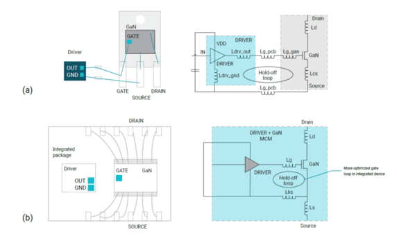
Example of parasitic effects in circuits
TI's LMG3650 integrates a 650V GaN FET. Currently, three different RDSons are provided, namely 25mΩ, 35mΩ, and 70mΩ. Different RDSons correspond to different power levels. A lower Rdson can support a relatively higher power level, and the COSS of a higher Rdson will be smaller. Suitable for scenarios with small conducted interference; And 35mΩ is suitable for scenarios with small switching interference.In terms of protection and sensing functions, the protection features include under-voltage locking (UVLO), periodic overcurrent limiting, short-circuit and overheat protection. The LMG365x provides a 5V LDO output on the LDO5V pin and can be used to power external digital isolators. The LMG3656R025 incorporates Zero Voltage Detection (ZVD) functionality, which can provide pulse output from the ZVD pin when achieving zero voltage switching. The LMG3657R025 features a zero current detection (ZCD) function, which can set the ZCD pin to a high level when the drain-source current is negative and switch to a low level when a zero-crossing point is detected.
Through the integration of power tubes, drivers and protection, TI's GaN achieves the best performance of ultra-high integration.
Full coverage from Grid to Gate
GaN of different voltage levels can be used to build a full coverage from AC to DC of different voltage levels. For example, use 650V GaN FET for AC/DC to DC/DC conversion, or use 100V or 200V GaN FET for DC/DC conversion.
You Shengyang introduced that, taking the PSU of the server power supply as an example, starting from the AC input, the first stage is the DC bus from AC to 400V or 450V. The DC bus from AC to 400V to 450V generally uses a bridge-free rectifier, and the LMG365x can be applied to the high-frequency switching on the bridge-free rectifier. The power level grades generally may include 1.8kW, 3.6kW, and even 8kW and 12kW. When the power level is relatively high, customers usually choose the multi-phase interlacing scheme.
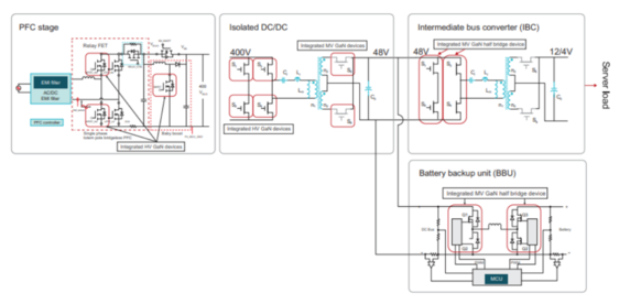
After rectification from AC/DC, there is an isolated DC/DC converter, generally ranging from 400V or 450V to 48V. Due to the current requirements for high power density and high efficiency, soft-switching topologies, such as LLC series resonant circuits, are often used. On soft-switching circuits, TI's gallium nitride can also provide a relatively low COSS, reducing the circulating current loss on the soft-switching LLC series resonant controller converter. The measured results show that TI's GaN devices with TOLL packaging can achieve an efficiency of over 99% at the PFC level and over 98% at the DC/DC level.
For medium-voltage Gans, the three main systems in server power supply applications can adopt Gans ranging from 100V to 200V:
Power Supply Unit (PSU) : Changes in the open computing project are heating up the 48V output. However, the losses (gate drive and overlap losses) of the required 80V and 100V silicon solutions have increased significantly compared to previous solutions. GaN solutions such as LMG3100 help minimize the aforementioned losses in the LLC secondary side synchronous rectifier as much as possible.
Intermediate Bus Converter (IBC) : This system converts the intermediate voltage (48V) output by the PSU to a lower voltage and then transmits it to the server. With the popularity of the 48V voltage level, IBC helps reduce the I 2R loss in the server subsystem and reduces the size and cost of busbars and power transmission lines. The drawback of IBC is that it adds an extra step in power conversion, which may have an impact on efficiency. Therefore, in addition to several new topologies that Oems have tested to achieve the best combination of high efficiency and high power density, GaN can also play a role.
Battery backup unit: The buck/boost stage typically converts the battery voltage (48V) to the bus voltage (48V). When the mains power line is cut off and the power flow is bidirectional, the BBU can also be used for battery power conversion. The reason why uninterruptible power supplies use this stage is that they perform a direct DC/DC conversion only once through the battery, avoiding the losses caused by DC/AC/DC conversion.
Summary
Power density within data centers is accelerating. About a decade ago, the average power density per rack was approximately 4 to 5 kW, but today's hyperscale cloud computing companies (such as Amazon, Microsoft, or Facebook) typically require a power density of 20 to 30 kW per rack. Some professional systems have even higher requirements, demanding that the power density of each rack reach over 100kW. Due to the limited space for power storage and heat dissipation, high power density requires compact and highly energy-efficient power supply design. At the same time, the power supply also needs to meet the specific requirements of the data center industry.
GaN is undoubtedly one of the most effective methods to increase power density. GaN can provide a higher switching frequency and lower power loss, and these advantages are particularly prominent in situations where power supply design is simplified and power density is improved. TI's standard TOLL package, fully integrated, covers both high-voltage and medium-voltage GaN products, making it highly suitable for full-scenario applications in data center power supplies.
免责声明: 本文章转自其它平台,并不代表本站观点及立场。若有侵权或异议,请联系我们删除。谢谢! Disclaimer: This article is reproduced from other platforms and does not represent the views or positions of this website. If there is any infringement or objection, please contact us to delete it. thank you! |

WeChat Official Account

WeChat Service
 Email
Email QQ
QQ 13823761625
