
USB has evolved from a data interface with limited power supply to an important power supply component with a data interface function. The latest USB 3.x protocol supports higher levels of power flux. The default voltage is 5V, and the USB-C port can "negotiate" with the inserted device to increase the port voltage to 20V.
A unique challenge in the new power requirements is how to use a 4.5V-32V input voltage to provide a 5V-20V DC bus. A 4-switch buck-boost converter is the right topology for buck or boost power conversion because it offers the wide voltage conversion range, positive polarity, high energy efficiency, and small size solutions that designers and customers need. On Semiconductor's NCP81239 4-switch Step-up-and-boost controller for USB-powered and USB-C applications drives up to four switches, enabling converters to step-down or step-up, and enables users to meet USB Power (PD) specifications for all USB PD applications, such as PC/laptop, mobile power, and expansion ports.
In synchronous buck converters, there is a well-known phenomenon, which is called "low end misinformation" or "dv/dt inductance conduction", which is the culprit of breakdown, potentially damaging the switch and reducing the reliability of the entire converter.
This problem is then doubled in the 4-switch buck-boost converter because it has two phases - buck and boost. Errors occur when designers copy the circuit parameters of the buck converter directly to the boost segment of the 4-switch buck - boost converter. As this topology becomes more and more popular in applications, it becomes more and more important to understand the dv/dt inductance conduction problem.
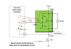
In 4-switch buck-boost converters, the dv/dt inductance turn-on is caused by the rapidly rising drain-source voltage of the synchronous rectified MOSFETs in the buck and boost segments. Due to unwanted breakdown current flowing through either phase of the bridge arm, the result is a decrease in the overall system energy efficiency. There are several economical circuit options available to power designers, including minimizing the turn-off gate drive resistance of the rectifier switch, increasing the on-gate drive resistance of the active switch, or adding an RC buffer circuit to the switching node. Choosing a MOSFET with a low Qgd/Qgs(th) ratio and a high threshold voltage also reduces the possibility of misdirection of dv/dt inductors.
免责声明: 本文章转自其它平台,并不代表本站观点及立场。若有侵权或异议,请联系我们删除。谢谢! Disclaimer: This article is reproduced from other platforms and does not represent the views or positions of this website. If there is any infringement or objection, please contact us to delete it. thank you! |

WeChat Official Account

WeChat Service
 Email
Email QQ
QQ 13823761625
