
Motor drive circuit
Feature:Does the motor run one way or two ways? Do you need speed regulation? For unidirectional motor drive, as long as a high-power transistor or field effect tube or relay directly drive the motor, when the motor needs to be bidirectional rotation, you can use the H-bridge circuit composed of 4 power components or use a double-pole double-throw relay. If speed regulation is not required, just use a relay; However, if speed regulation is required, switching elements such as triode and field effect tube can be used to achieve PWM (pulse width modulation) speed regulation.
property:For PWM speed control motor drive circuit, there are mainly the following performance indicators.
1) Output current and voltage range, which determines how much power the circuit can drive the motor.
2) Efficiency, high efficiency not only means saving power, but also reduces the heat of the drive circuit. To improve the efficiency of the circuit, you can start with ensuring the switching status of the power device and preventing common-mode conduction (a problem that may occur in H-bridge or push-pull circuits, that is, two power devices are switched on at the same time to short-circuit the power supply).
3) Influence on the control input. The power circuit should have good signal isolation to its input to prevent high voltage and high current from entering the main control circuit, which can be isolated by high input impedance or photoelectric coupler.
4) Influence on power supply. The common-mode conduction can cause the instantaneous drop of the power supply voltage and cause the pollution of the high-frequency power supply. Large currents may cause ground potential to float.
5) Reliability. The motor drive circuit should be as far as possible, no matter what kind of control signal, what kind of passive load, the circuit is safe.
Triode - resistor as grid driver
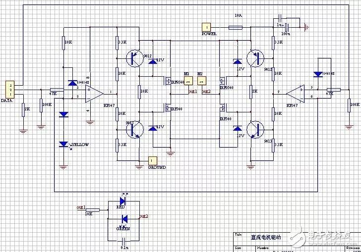
1, input and level conversion part:
The input signal cable is introduced by DATA. Pin 1 is the ground cable, and the rest is the signal cable. Note that pin 1 is connected to ground with a 2K ohm resistor. When the driver board and the MCU are powered separately, this resistor can provide the signal current reflux path. When the driver board and the single chip microcomputer share a set of power supplies, this resistance can prevent large current along the line into the single chip microcomputer motherboard ground wire interference. In other words, it is equivalent to separating the ground wire of the driver board from the ground wire of the single-chip computer to achieve "one point of grounding".
The high-speed op amp KF347 (also TL084) acts as a comparator, comparing the input logic signal with the 2.7V reference voltage from the indicator and a diode to convert it into a square-wave signal close to the voltage amplitude of the power supply. The input voltage range of the KF347 should not be close to the negative supply voltage, otherwise an error will occur. Therefore, a diode is added at the op-amp input to prevent the voltage range from overflowing. The two resistors at the input are used to limit the current and to pull the input to a low level when the input is suspended.
It is not possible to replace the opamp with the LM339 or any other open-output comparator, because the high-level output impedance of the open output is above 1000 ohm, and the voltage drop is large, and the subsequent triode will not be able to cut off.
2. Grid drive part:
The circuit composed of the rear triode, resistor, and regulator tube further amplifies the signal, drives the gate of the FET and uses the gate capacitance of the FET itself (about 1000pF) for delay to prevent the FET of the upper and lower arms of the H-bridge from simultaneously conducting (" common-state conducting "), resulting in short circuit of the power supply.
When the output end of the op amplifier is low (about 1V to 2V, can not fully reach zero), the following triode is cut off, and the field effect tube is on. The above triode is on, the FET is off, and the output is high. When the op amp output is high (about VCC- (1V to 2V), can not fully reach VCC), the following triode conduction, FET cut-off. The above triode is off, the FET is on, and the output is low.
The above analysis is static, and the dynamic process of switching is discussed below: the on-resistance of the triode is much less than 2,000 ohm, so the charge on the gate capacitor of the FET can be released quickly when the triode is converted from the cutoff to the on-conduction, and the FET is quickly cut off. However, it takes a certain amount of time for the triode to charge the FET grid through the 2,000 ohm resistance when it is converted from conduction to cutoff. Accordingly, the speed of conversion from conduction to cutoff is faster than the speed of conversion from cutoff to conduction. If the switching action of the two triodes occurs at the same time, this circuit can make the field effect tubes of the upper and lower arms break first and then open, eliminating the common mode conduction phenomenon.
In fact, it takes a certain amount of time for the output voltage of the op amp to change, and during this time the output voltage of the op amp is in the middle value between the positive and negative supply voltage. At this time, the two triodes are simultaneously conducting, and the FET is cut off at the same time. So the actual circuit is a little safer than this ideal.
The 12V voltage regulator diode of the FET grid is used to prevent overvoltage breakdown of the FET grid. The general grid voltage of the FET is 18V or 20V, and directly adding 24V voltage will break down, so this voltage regulator can not be replaced by an ordinary diode, but can be replaced by a resistance of 2,000 ohms, and can also get a partial voltage of 12V.
3. Fet output part:
There is a diode in reverse parallel between the source and the drain inside the high-power FET, and when it is connected to the H-bridge, it is equivalent to the four diodes used to eliminate voltage spikes in parallel at the output end, so there is no external diode here. The output end is paralleled with a small capacitor (between out1 and out2) to reduce the peak voltage generated by the motor has a certain benefit, but when using PWM there is a side effect of spiking current, so the capacity should not be too large. This capacitance can be omitted when using a low-power motor. If you add this capacitor, be sure to use a high voltage resistance, ordinary porcelain capacitor may occur breakdown short circuit fault.
The circuit composed of resistor, LED and capacitor with parallel output indicates the direction of motor rotation.
4. Performance index:
Power supply voltage 15~30 V, the maximum continuous output current 5A/ each motor, a short time (10 seconds) can reach 10A, PWM frequency can be used up to 30KHz (generally 1 to 10KHz). The circuit board consists of four logically independent power amplifier units, whose output ends are connected to H bridge in pairs, which can be controlled directly by single chip microcomputer. To realize the motor bidirectional rotation and speed regulation.
5. Wiring:
The high current line should be as short and thick as possible, and try to avoid passing through the hole. If you must pass through the hole, make the hole larger (" 1mm ") and make a circle of small passing holes on the pad. Fill it with solder when welding, otherwise it may burn out. In addition, if a voltage regulator is used, the field effect tube source pole should be as short and thick as possible to the power and ground wires, otherwise at high current, the voltage drop on this section of the wire may be burned by the positive bias regulator tube and the on-transistor. In the original design, a 0.15ohm resistor was connected between the source pole of the NMOS tube to detect the current, and this resistor became the culprit of constantly burning the board. Of course, if the regulator is replaced by a resistor, this problem does not exist.
Simple gate drive for low voltage drive circuits
The maximum gate-source voltage of the general power FET is about 20V, so it is necessary to ensure that the gate-source voltage cannot exceed 20V in 24V applications, which increases the complexity of the circuit. However, in the application of 12V or lower voltage, the circuit can be greatly simplified.
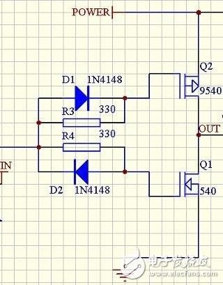
Above is one side of a 12V drive axle, where the triode portion of the circuit is replaced by two diodes and two resistors. (Note that the logic of the previous figure is reversed) Due to the presence of the grid capacitor of the FET, charging the grid capacitor through R3 and R4 makes the FET delay the conduction; By directly discharging the gate capacitor through the diode, the FET is immediately cut off, thus avoiding common-state conduction.
L298N motor drive circuit
1. Analysis of working principle:
In the stepper motor drive module, TLP521 with optocoupler isolation and strong anti-interference ability is used as the isolation current protection chip, in which the 17 pin of L297 controls the positive and negative rotation of the stepper motor by giving the high and low level, and the 18 pin is the input end of the stepper clock to control the time increment of each step, and the selection of half step or whole step of the 19-step stepper motor. The 10-pin is the enable control terminal to control the start and stop of the motor, and the positive and negative rotation of the motor is controlled through the internal 4-channel logic drive circuit, high voltage and high current double H bridge driver L298; The use of L298 to achieve motor drive and reverse rotation, and the use of diodes for continuous current protection, the use of 7805 to provide 5v power supply to the controller and l298 chip power supply, this circuit is easy to heat in the case of long working time, resulting in circuit instability.
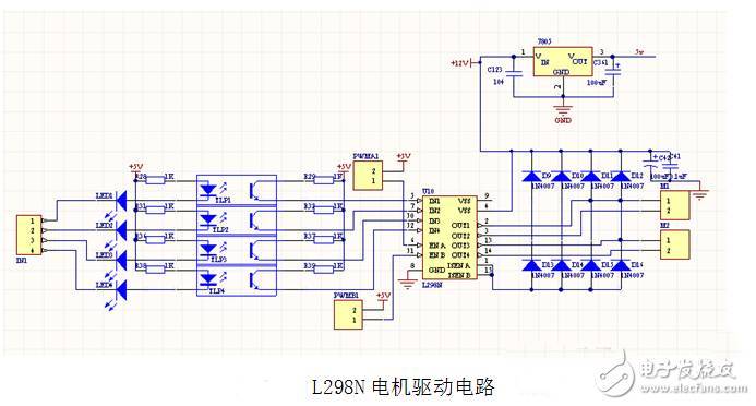
The main functional features are:
Key chip: L298N double H-bridge DC/stepper motor driver chip
L298N chip operating voltage: DC 4.5~5.5V.
Motor drive power supply voltage DC 5--35V.
When the power input is normal, the LED light indicates.
PCB size: 4.4*5.0cm
Maximum output current 2A (instantaneous peak current 3A), maximum output power 25W.
When the output is normal, the motor operation is indicated by LED light.
With diode continuous current protection.
Two DC motors or one two-phase 4-wire (or 6-wire) stepper motor can be individually controlled.
A DC motor up to 3A can be controlled using the parallel coupling method.
Can realize the motor positive and negative rotation.
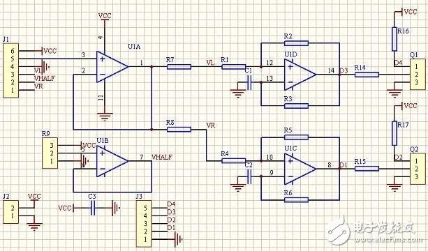
2. Analog circuit PWM implementation
Brief summary
This paper mainly introduces the design of motor drive circuit. The circuit realized by this scheme can adopt independent single chip microcomputer or CPLD plus field effect tube drive circuit and current sampling feedback circuit.
免责声明: 本文章转自其它平台,并不代表本站观点及立场。若有侵权或异议,请联系我们删除。谢谢! Disclaimer: This article is reproduced from other platforms and does not represent the views or positions of this website. If there is any infringement or objection, please contact us to delete it. thank you! |

WeChat Official Account

WeChat Service
 Email
Email QQ
QQ 13823761625
