Main points of this article
PCB wiring has inductance and capacitance, which together determine the impedance of the wiring.
Sometimes it is helpful to know the inductance of the track to estimate the coupling due to crosstalk.
Although no specific line inductance value is set, it is a powerful tool for understanding signal behavior in some systems.
All PCB wiring has some inductance, but do you know how inductance in PCB wiring affects electrical behavior? The different conductor systems in the PCB need to have a specific line width, which will determine the inductance of the line. However, there is no specific PCB wire inductance rule of thumb, only the calculation formula related to the wire impedance can be used to determine the wire inductance. In addition, there are no specific regulations that require us to use specific wiring inductors as design goals in board design.
With an understanding of the important factors that determine the input impedance of the wiring, it is easier to determine when you can deviate from the impedance target and choose a higher or lower wiring impedance in the board design.
PCB inductance rule of thumb
In the design of transmission line, the calculation of the width of the line often starts from the design of stacking and the selection of the transmission line geometry. Other systems, such as power converters, may not need to control impedance along the wires, so they will often use wider copper wires to reduce inductance. In the calculation of inductance, the impedance should be calculated first, and then the impedance is used to calculate the inductance of the line.
Impedance calculation formula
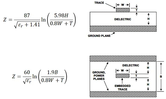
The most basic impedance model used by the PCB industry is the formula in the IPC-2141 standard. The IPC-2141 microstrip line and strip line impedance calculation formulas shown below are based on experimental observations and have high accuracy in the frequency range below 1GHz.

IPC-2141 microstrip line and strip line impedance calculation formula is found to have high accuracy in the frequency range below 1GHz.
As it turns out, the above formula is not entirely accurate and contains some assumptions that do not always hold. Specifically, the above formula has the following flaws:
Ignore the loss Angle tangent: All PCB laminates will produce a certain attenuation, this value can be quantified using the loss Angle tangent. The tangent of the loss Angle usually increases the reactance, causing a slight change in the line impedance.
Copper roughness: Skin effects and copper roughness have been integrated into the above formula and cannot be separated separately without a more complex approach (such as the IEEE model). Therefore, the above formula does not apply to all manufacturing processes and material systems.
Although the above formulas are not perfect, they provide a good starting point for calculating the line impedance and are suitable for many situations in PCB design.
Calculate the inductance based on the impedance
After the track width is designed to meet the impedance target, the track will have a specific inductance. The design process is generally not done in reverse unless it involves low-speed digital signals, low-frequency analog signals, or switching power converters with specific low inductance requirements. If the track length is short enough, the typical 50 ohm impedance target can be appropriately deviated at design time, using a lower track inductance.
In summary, there is no rule of thumb for PCB wiring inductance. In other words, there is no specific wiring inductance requirement, and there is no simple formula to calculate the wiring inductance of all PCBS.
To explore further, we can again refer to the IPC-2141 calculation formula and the constitutive impedance relationship of a lossless transmission line. The IPC-2141 equation contains a formula for calculating capacitance per unit length, which can be used to calculate PCB wiring inductance.

Microstrip line and strip line capacitors
In the specific configuration described above, the wiring capacitance is defined with respect to the nearest ground plane. Finally, we obtain two formulas for calculating the inductance of microstrip line and strip line respectively.

Microstrip line and strip line inductance
From this we can see that the wiring inductance depends on:
. Wire thickness (or copper weight)
Layer thickness
. Cable geometry
To ensure that the design meets the impedance objective and determines the inductance, both of these factors must be considered. When calculating inductance, the layer thickness (H or B) and copper weight (T) are usually fixed, and the impedance and/or wiring density targets need to be met by determining the wiring width. When designing the wiring on a stack using a particular laminate material, the inductance or impedance will vary if the same wiring is placed in a PCB stack using a different dielectric material. If necessary, various stacks of inductance and width curves can be compared.
Limitations of PCB wiring inductance rules
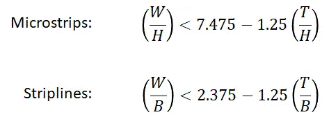
Because the above equation is a logarithmic equation, it is only valid within a certain range of values of the geometric parameters. As long as the parameter in the above logarithm is less than 1, the calculated inductance is negative. By rewriting the parameters in the logarithm as ratios (W/H) or (W/B), and (T/H) or (T/B), we derive the following inequality, which limits the allowable linear geometry in the above formula:

In order for the inductance of IPC-2141 to be non-negative, it is necessary to restrict the geometry of the microstrip and strip lines
For example, we can observe microstrip line inductance in a simple PCB stack with impedance control. On a four-layer board using 0.5 oz/sf copper wiring (dielectric thickness 8mil, Dk=4.2), the required wiring width to obtain a 50Ohm impedance is 15.15mil and the inductance is 6.679nH/ inch. Other models have produced very different results, which is enough to show that IPC-2141 is flawed.
In addition to using the outdated IPC-2141 formula, there are better ways to determine the impedance and inductance of the track. More efficient PCB stacking and routing calculators include moment method field solvers or boundary element method field solvers. These tools can be used to quickly calculate the PCB wiring inductance on the board for a given layering and impedance target, and then use that inductance value to determine rough crosstalk results. Some very sensitive precision measurement designs or power converters require very low inductive wiring, and these calculations can be validated as a reference.
Cadence's PCB design and analysis software can be used to validate any PCB routing inductance rule of thumb when evaluating advanced electronic designs. Designers can use powerful field solvers and circuit modeling tools to simulate electrical behavior and calculate many important signal integrity metrics. When using Cadence's software suite, we also have access to a range of simulation capabilities that can be used for signal integrity analysis to fully evaluate system functionality.
免责声明: 本文章转自其它平台,并不代表本站观点及立场。若有侵权或异议,请联系我们删除。谢谢! Disclaimer: This article is reproduced from other platforms and does not represent the views or positions of this website. If there is any infringement or objection, please contact us to delete it. thank you! |


