3.3V powered STM32 development board, output 24V industrial sensor, if the two are directly connected together, what will happen? Have you ever done something similar by connecting different levels of chips or development boards? Fortunately, the signal can not be read, which may cause the chip or development board to burn directly.
At this point, a "mediator" is needed. This period of trade ze science laboratory, to talk about the level conversion of this "mediator" -
Why level switching
In our usual design, we often encounter the following two situations that require level conversion:
1) Voltage mismatch
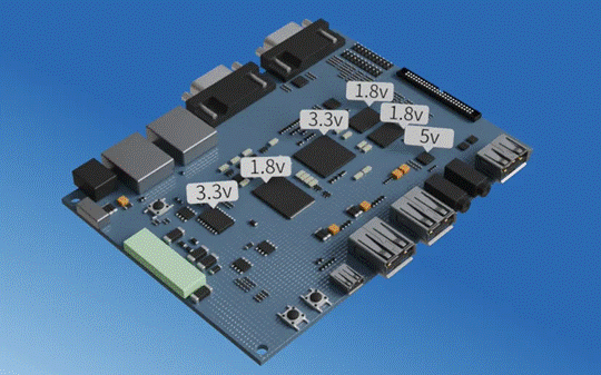
In digital circuits and embedded systems, different chips or modules may use different voltage standards, such as 1.8V, 3.3V, 5V, 12V, 24V, etc. When these chips or modules with different voltages need to communicate, if directly connected, it may cause signal transmission confusion and even damage the chip. Therefore, level switching is required to ensure that the signal can be correctly transmitted between different voltage systems.
2) Incompatible logic levels
In addition to voltage mismatch, there are also incompatibilities between different logic level standards (such as TTL, CMOS, LVCMOS, etc.). These logic level standards have different voltage ranges and logic level definitions, so they need to be converted accordingly to ensure the correct transmission and processing of the signal. Level switching enables conversion between different logic level standards to address compatibility
Voltage mismatch level switching
There are three main cases of voltage mismatch:The first: the digital I/O port of the chip does not match the level of the external module, that is, the single chip microcomputer and the sensor at the beginning of the video, and the output level of the sensor or driver does not match the I/O level of the single chip microcomputer.
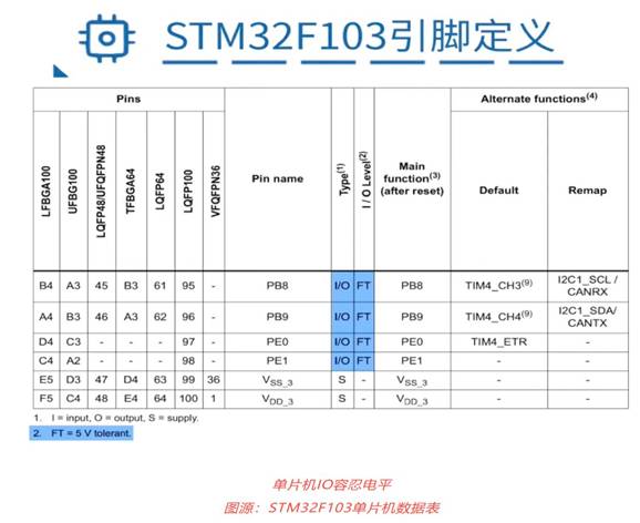
For example, some industrial sensors use 24V power supply, if the MCU wants to collect sensor data, then the IO port of the MCU must be able to withstand 24V voltage, but now most of the MCU is 3.3V power supply, then the IO port is certainly not able to withstand 24V, this time, It is necessary to add a level conversion circuit between the sensor and the MCU to convert the 24V signal into the level range that the MCU can tolerate.
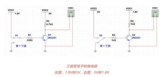
Take 1.8V to 5V as an example, when the switch S1 is connected to 1.8V, Q1 is switched on and the voltage of Q1 collector is 0V; when S1 is grounded, Q1 is cut off and the voltage of Q1 collector is 5V, and the same is true for 5V to 1.8V.
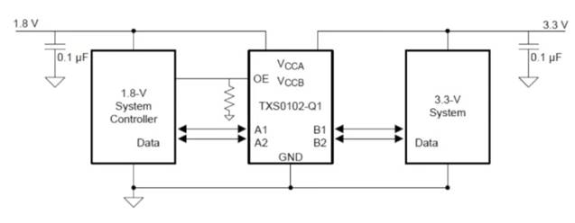
The advantage of using triode conversion is that the circuit is simple, the cost is low, and there are disadvantages, the communication speed is limited by the switching speed of the triode, and the communication speed is too low. If you need high-speed communication, you need to use a special high-speed level conversion chip, such as TI's TXS0102DCUR, which can convert 2 levels at the same time, and the conversion rate can be as high as 24Mbps in push-pull mode. Of course, different conversion channels or conversion rates have specialized chips that can be used.
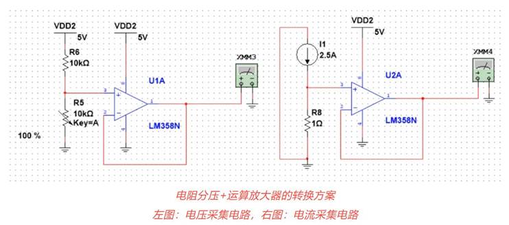
Second: The analog I/O port of the chip does not match the external analog range.
Common is ADC data conversion, the effective input range of MCU analog I/O is 0-VRef, when the analog signal input exceeds VRef or exceeds the chip VDD voltage, it will cause range overflow or analog I/O port permanent damage, and the analog output we use is a variety of patterns. For example, 0~5V, -2.5V~2.5V, 0~10V or 4~20mA signals, etc., at this time, it is necessary to convert these external analog quantities into 0~VRef signals that can be measured by the MCU. The door's high-speed level conversion chips, such as TI's TXS0102DCUR, can convert 2 levels simultaneously, with a conversion rate of up to 24Mbps in push-pull mode. Of course, different conversion channels or conversion rates have specialized chips that can be used.

The third: the communication interface conversion of the chip.
Commonly used communication protocols, such as RS485, RS232, CAN, have different level standards, these communication levels are not integrated in the MCU, if you want to use these communication methods, you need to use level co
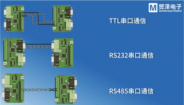
The conversion of the communication interface is very simple, and the corresponding communication chip can be directly selected. For example, RS485 communication CAN choose MAX485, RS232 can use MAX232, CAN can choose SN65HVD230DR, the program is basically fixed, according to the corresponding chip data manual design circuit is no problem.
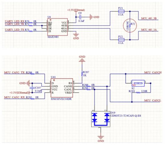
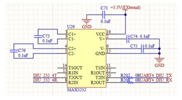
Logic level incompatible level switching
Logic level, the voltage level used to represent the state of a digital signal. In digital systems, binary 1s and 0s are represented by logic levels, with high logic levels usually represented as 1 and low logic levels usually represented as 0. The stability of the logic level is essential for the correct recognition and processing of digital signals.
There are two widely known logic levels: TTL logic level and CMOS logic level. The full name of TTL logic level is transistor-transistor integrated logic level, such as some of the 74 series chips we use now, it is TTL level. The CMOS logic level is the complementary symmetric metal oxide semiconductor logic level. It usually means that many devices in the circuit are composed of PMOS transistors or NMOS transistors.
Both TTL and CMOS have their own logic level standards, that is, the level corresponding to 1 and 0.
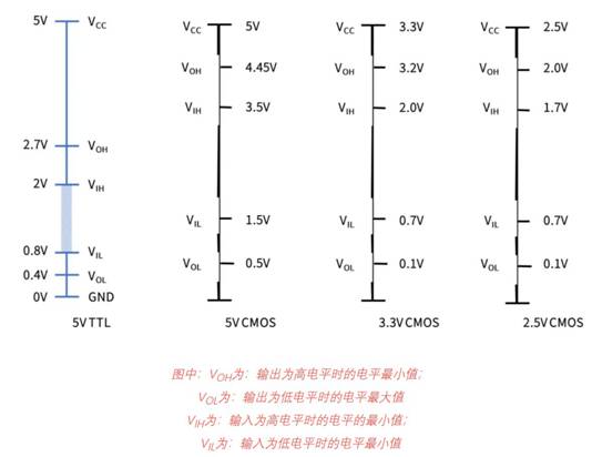
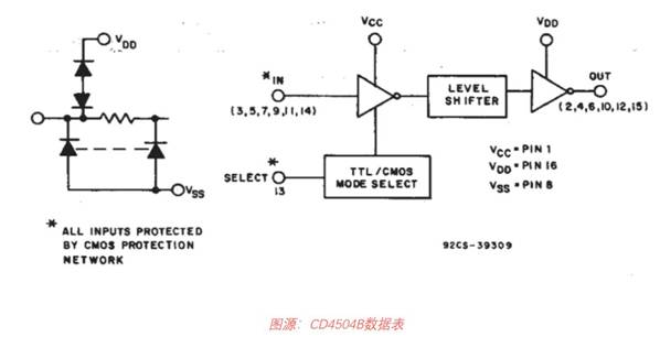
As can be seen from the figure above, there are differences between TTL logic level and CMOS logic level, but through analysis, we found that their level is compatible in a certain range, since it is compatible, it can not be converted, this is not possible, here for example, to 5VTTL and CMOS comparison, such as a signal rate of 10GHZ, In TTL level, the high level is determined to be more than 2V, and in CMOS level, the high level is determined to be more than 3.5V, the difference between 1.5V, we all know that the rise of the signal takes time, at the rate of 10G, the time difference of the confirmation level is very important, this time difference will cause the signal timing error. Eventually, the signal transmission fails, so the TTL and CMOS logic level also need to be converted, usually TTL to CMOS need to use a special conversion chip, such as CD4504B, it can achieve TTL to CMOS.
Whether it is a voltage mismatch level conversion, or a level conversion between logical levels, there are many forms of conversion, the above is just one of the ways, but as long as the purpose of level conversion is to make the level compatible, what conversion is OK.
Although these level switching circuits are not complex, they still require additional device construction. Is it possible to integrate the conversion circuit into the MCU or improve the I/O voltage? This is related to the low power consumption and high speed of the MCU, low voltage can bring less loss, if you add these conversion circuits, it will increase power consumption, but also reduce the flexibility of the chip. Since it cannot be integrated into the interior, then the question comes again, why not unify the level standards? This is a good question, as the world's charging plug can not be unified, each chip has its own standards, unification is really difficult.
免责声明: 本文章转自其它平台,并不代表本站观点及立场。若有侵权或异议,请联系我们删除。谢谢! Disclaimer: This article is reproduced from other platforms and does not represent the views or positions of this website. If there is any infringement or objection, please contact us to delete it. thank you! |


