
Mosfets are widely used in both analog and digital circuits and are closely related to our lives. The advantages of MOSFET lie in the following: Firstly, the driving circuit is relatively simple. The driving current required by MOSFET is much smaller than that of BJT, and it can usually be directly driven by CMOS or collector open-circuit TTL driving circuits. Secondly, the switching speed of MOSFET is relatively fast and it can operate at a high speed because there is no charge storage effect. In addition, MOSFETs do not have a secondary breakdown failure mechanism. They tend to have stronger endurance at higher temperatures, and the possibility of thermal breakdown is lower. They can also provide better performance over a wide temperature range. Mosfets have been widely applied and can be found everywhere in consumer electronics, industrial products, electromechanical equipment, smart phones and other portable digital electronic products.
In recent years, with the rapid development of industries such as automobiles, communications, energy, consumer goods, and green industries, which widely apply MOSFET products, power MOSFETs have attracted much attention. It is predicted that the overall compound annual growth rate of China's power MOSFET market will reach 13.7% from 2010 to 2015. Although market research firm iSuppli stated that the power MOSFET market would slow down this year due to macro investment and economic policies as well as wafer and raw material supply issues caused by the earthquake in Japan, the demand for consumer electronics and data processing remains strong. Therefore, in the long term, the growth of power MOSFETs will continue for a considerable period of time.
Technology has been advancing continuously, and the power MOSFET market has gradually been challenged by new technologies. For instance, many companies in the industry have already begun to develop GaN power devices and assert that the space for performance improvement of silicon power MOSFETs is already very limited. However, the challenge that GaN poses to the power MOSFET market is still in a very early stage. Mosfets still hold obvious advantages in terms of technological maturity and supply volume. After more than three decades of development, the MOSFET market will not be easily and rapidly replaced by new technologies.
Mosfets will still hold a dominant position for five years or even longer. MOSFET will still be a device that many newly entered engineers will come into contact with. This issue of the Half-monthly Talk will start from the basics and explore some fundamental knowledge of MOSFET, including selection, introduction of key parameters, considerations of the system and heat dissipation, etc. Finally, I will also introduce some of the most common and popular applications to everyone.
The selection basis of MOSFETs
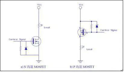
There are two major types of MOSFETs: N-channel and P-channel. In power systems, MOSFETs can be regarded as electrical switches. When a positive voltage is applied between the gate and the source of an N-channel MOSFET, its switch conducts. When conducting, the current can flow through the switch from the drain to the source. There exists an internal resistance between the drain and the source, which is called the on-resistance RDS (ON). It must be clear that the gate of a MOSFET is a high-impedance terminal. Therefore, a voltage always needs to be applied to the gate. If the gate is floating, the device will not function as designed and may conduct or turn off at inappropriate times, resulting in potential power loss in the system. When the voltage between the source and the gate is zero, the switch is turned off and the current stops flowing through the device. Although the device has been turned off at this time, there is still a tiny current existing, which is called leakage current, or IDSS.
As the basic components in the electrical system, how do engineers make the right choices based on parameters? This article will discuss how to select the correct MOSFET through four steps.
1) Selection of channels. The first step in choosing the right device for the design is to decide whether to use an N-channel or P-channel MOSFET. In a typical power application, when a MOSFET is grounded and the load is connected to the main line voltage, this MOSFET constitutes a low-voltage side switch. In the low-voltage side switch, an N-channel MOSFET should be adopted, which is based on the consideration of the voltage required to turn off or on the device. When the MOSFET is connected to the bus and grounded to the load, a high-voltage side switch should be used. P-channel MOSFETs are usually adopted in this topology, which is also due to the consideration of voltage drive.
2) Selection of voltage and current. The higher the rated voltage is, the higher the cost of the device will be. Based on practical experience, the rated voltage should be greater than the main line voltage or bus voltage. Only in this way can sufficient protection be provided to prevent the MOSFET from failing. When choosing a MOSFET, it is necessary to determine the maximum voltage that can be endured between the drain and the source, that is, the maximum VDS. Other safety factors that design engineers need to consider include voltage transients induced by switching electronic devices such as motors or transformers. The rated voltages for different applications also vary. Generally, portable devices are 20V, FPGA power supplies are 20-30V, and 85-220VAC applications are 450-600V.
In the continuous conduction mode, the MOSFET is in a steady state, and at this time, the current continuously passes through the device. A pulse spike refers to a large amount of power surge (or peak current) flowing through the device. Once the maximum current under these conditions is determined, it is only necessary to directly select the device that can withstand this maximum current.
3) Calculate the conduction loss. The power loss of MOSFET devices can be calculated by Iload2×RDS (ON). Since the on-resistance varies with temperature, the power loss will also change proportionally. For portable designs, it is easier (more common) to adopt a lower voltage, while for industrial designs, a higher voltage can be used. Note that the RDS (ON) resistance will rise slightly with the current. The variations of various electrical parameters regarding the RDS (ON) resistance can be found in the technical data sheet provided by the manufacturer.
4) Calculate the heat dissipation requirements of the system. Designers must consider two different situations, namely the worst-case scenario and the actual situation. It is recommended to adopt the calculation results for the worst-case scenario, as this result provides a greater safety margin and can ensure that the system does not fail. There are still some measurement data that need attention on the MOSFET data sheet. For instance, the thermal resistance between the semiconductor junction of the packaged device and the environment, as well as the maximum junction temperature.
Switching loss is actually also a very important indicator. As can be seen from the following figure, the product of voltage and current at the moment of conduction is quite large. To a certain extent, it determines the switching performance of the device. However, if the system has relatively high requirements for switching performance, a power MOSFET with a relatively small gate charge QG can be selected.
Analysis of MOSFET Application Cases
1. Switching power supply application
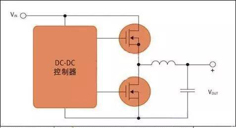
By definition, this application requires MOSFETs to be turned on and off regularly. Meanwhile, there are dozens of topologies available for switching power supplies. Here, we consider a simple example. The basic step-down converter commonly used in DC-DC power supplies relies on two MOSFETs to perform the switching function (as shown in the figure below). These switches alternately store energy in the inductor and then release the energy to the load. At present, design staff often choose frequencies of several hundred kHz or even above 1 MHz, because the higher the frequency, the smaller and lighter the magnetic components can be. The second most important MOSFET parameters in a switching power supply include output capacitance, threshold voltage, gate impedance and avalanche energy.
2.Motor control application
Motor control applications are another field where power MOSFETs can play a significant role. A typical half-bridge control circuit uses two MOSFETs (while a full-bridge circuit uses four), but the turn-off times (dead time) of these two MOSFETs are equal. For this type of application, the reverse recovery time (trr) is very important. When controlling an inductive load (such as a motor winding), the control circuit switches the MOSFET in the bridge circuit to the off state. At this time, another switch in the bridge circuit temporarily conducts current in reverse through the body diode in the MOSFET. Thus, the current circulates again and continues to supply power to the motor. When the first MOSFET conducts again, the charge stored in the other MOSFET diode must be removed and discharged through the first MOSFET, which is an energy loss. Therefore, the shorter the trr, the smaller this loss.
3.Automobile application
Over the past nearly 20 years, power MOSFETs for automobiles have made considerable progress. The power MOSFET is selected because it can withstand the transient high-voltage phenomena often encountered in automotive electronic systems, such as load drop and sudden changes in system energy. Moreover, its packaging is simple, mainly using TO220 and TO247 packages. Meanwhile, applications such as power Windows, fuel injection, intermittent wipers and cruise control have gradually become standard features of most cars, and similar power devices are needed in the design. During this period, with the increasing popularity of motors, solenoids and fuel injectors, automotive power MOSFETs have also continued to grow and develop.
The MOSFET devices used in automotive equipment cover a wide range of voltages, currents and on-resistance. The bridge configuration of the motor control equipment will use 30V and 40V breakdown voltage models. In situations where it is necessary to control the sudden unloading and sudden lifting of the load during startup, a 60V device will be used to drive the load. When the industry standard is transferred to 42V battery systems, 75V technology needs to be adopted. Equipment with high auxiliary voltage requires models ranging from 100V to 150V. As for MOSFET devices above 400V, they are applied in the control circuits of engine drive units and high-brightness discharge (HID) headlights.
The driving current range of automotive MOSFETs is from 2A to over 100A, and the on-resistance range is from 2mΩ to 100mΩ. The loads of MOSFET include motors, valves, lamps, heating components, capacitive piezoelectric components and DC/DC power supplies. The range of switching frequencies is usually from 10kHz to 100kHz. It must be noted that motor control is not suitable for switching frequencies above 20kHz. Other major requirements are UIS performance, operating conditions at the node temperature limit (-40 ° C to 175 ° C, sometimes up to 200 ° C), and high reliability beyond the vehicle's service life.以上翻译结果来自有道神经网络翻译(YNMT)· 通用场景
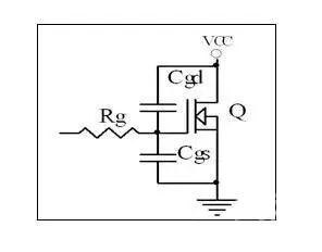
The switching speed of a MOSFET is closely related to the charging and discharging of its input capacitor. Although the user cannot reduce the value of Cin, they can lower the internal resistance Rs of the signal source in the gate drive circuit, thereby reducing the charge and discharge time constant of the gate circuit and accelerating the switching speed. Generally, the driving capability of an IC is mainly reflected here. When we talk about choosing a MOSFET, we mean using an external MOSFET to drive a constant current IC. Ics with built-in MOSFETs, of course, don't need to be considered by us. Generally, when the current is greater than 1A, external MOSFETs will be taken into account. To achieve greater and more flexible LED power capacity, an external MOSFET is the only option. The IC needs appropriate driving capability, and the MOSFET input capacitance is a key parameter. The Cgd and Cgs in the following figure are the equivalent junction capacitors of the MOSFET.
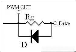
The PWM OUT output of a general IC integrates a current-limiting resistor internally. The specific value is related to the peak drive output capability of the IC and can be approximately regarded as R=Vcc/Ipeak. Generally, the Rg is selected around 10-20Ω in combination with the IC driving capability.
In general applications, the driver of an IC can directly drive a MOSFET. However, considering that the drive traces are usually not straight, the inductance may be larger. Moreover, to prevent external interference, an Rg drive resistor should still be used for suppression. Considering the influence of the distributed capacitance of the trace, this resistor should be as close as possible to the gate of the MOSFET.
The above discussion is about the selection of resistance when the MOSFET is in the ON state. When the MOSFET is in the OFF state, to ensure the rapid discharge of the gate charge, the resistance value should be as small as possible at this time. Usually, to ensure rapid discharge, a diode can be connected in parallel to the Rg. When the discharge resistance is too small, resonance may also occur due to the inductance of the trace (hence in some applications, a small resistor is also connected in series with this diode). However, since the reverse current of the diode does not conduct, the Rg participates in the reverse resonance circuit at this time, thus suppressing the peak of reverse resonance.
When estimating the conduction loss, output requirements and junction temperature, the methods pointed out in the previous text can be referred to.
The application fields of MOSFETs are extremely extensive and far beyond being summarized in just one or two articles.
Disclaimer: This article is reproduced from other platforms and does not represent the views or positions of this website. If there is any infringement or objection, please contact us to delete it. thank you! |

WeChat Official Account

WeChat Service
 Email
Email QQ
QQ 13823761625
