
Synchronous buck converters have been recognized as isolated bias power supplies in the communications and industrial markets. Isolated buck converters, or Fly-Buck converters as they are commonly called, use a coupled inductor instead of a buck converter inductor to create isolated as well as non-isolated buck outputs. Each isolated output requires only one winding, one rectifier diode and one output capacitor. This topology can be used to generate multiple semi-regulated isolated or non-isolated outputs in a simple and low-cost manner.
There are some major current differences between buck converters and Fly-Buck converters. We are already familiar with the switching current loop in buck converters, as shown in Figure 1. An input loop containing input bypass capacitors, VIN pins, high-low side switches, and ground return pins carries the switching current. The loop should be optimized for quiet operation to achieve a minimum trace length and a minimum loop area. The output loop containing the low-side switches, inductors, output capacitors, and ground return path actually carries the low-ripple DC current. While it is important to keep all current paths as short as possible to achieve low DC voltage drops, low losses, and low voltage regulation errors, the area of this loop is not as important as the input current loop.
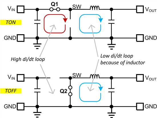
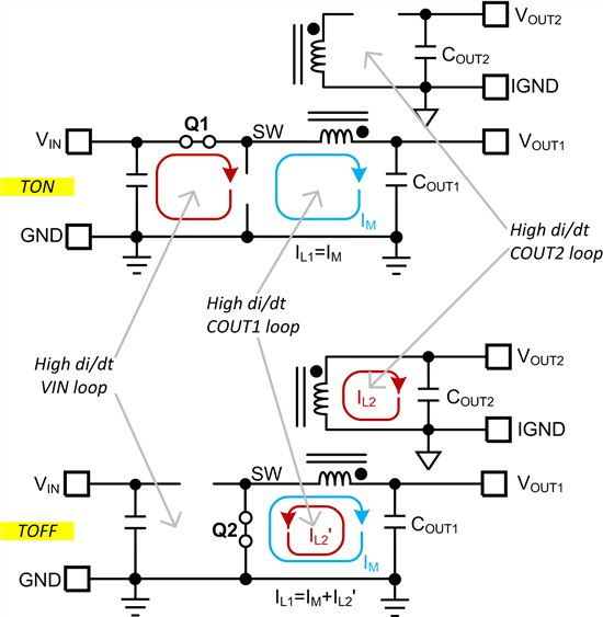
Figure 3 is an example of a layout that incorporates the guidance in this article. Like the switching node area, the high di/dt loops on the primary and secondary sides can also be minimized.
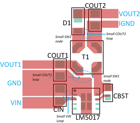
FIG. 3. The Fly-Buck layout based on LM5017 minimizes the area of di/dt loops and high di/dt SW1,2 nodes.
免责声明: 本文章转自其它平台,并不代表本站观点及立场。若有侵权或异议,请联系我们删除。谢谢! Disclaimer: This article is reproduced from other platforms and does not represent the views or positions of this website. If there is any infringement or objection, please contact us to delete it. thank you! |

WeChat Official Account

WeChat Service
 Email
Email QQ
QQ 13823761625
