
Introduction: High frequency high power switches in DC-DC converters may generate interference signals. Conducted noise on the input power line can be differential mode or common mode noise current formation.
High frequency high power switches in DC-DC converters may generate interference signals. Conducted noise on the input power line can be differential mode or common mode noise current formation. Mainly low frequency differential mode noise, fundamental switching frequency and harmonic frequency present on the input inductance. Common mode noise mainly has a high frequency component, measured between the converter input inductor and ground, similarly, the output of the switching DC-DC converter contains some kind of noise and ripple. Properly designed and implemented EMI(Electromagnetic interference) filtering can reduce noise to acceptable limits.
In Europe and the United States, conducted noise emission is limited by FCC and VDE standards ClassA and ClassB, and in all European countries, equipment used in homes and factories is required to meet the VDEClassB standard. In the United States, the FCC requires factory equipment to comply with ClassA, while home equipment is subject to the more stringent ClassB standard.
EMI filter scheme for reducing input noise
At present, most switching power supplies operate in the frequency range of 100KHz~1MHz, and the main peak of the conducted noise spectrum reflected back to the power supply corresponds to the fundamental switching frequency and its harmonic component. Conducted emission standards (e.g. EN55011, EN55022) specify the quasi-peak and average limit of conducted noise reflected from the input of the converter or power system to the source in the frequency range of 150KHz to 30MHz. To comply with this standard, all peaks in the conducted noise spectrum must be below a specific limit.
Element and sealed filtering scheme
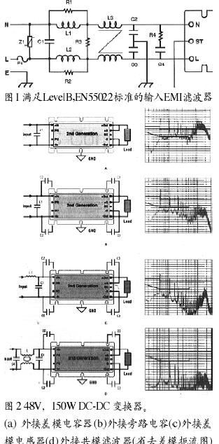
EMI filters are often in a single package, the configuration of which is shown in Figure 1. The EMI filter is a through-hole filter with a common mode choke diagram, Y capacitors (wire-to-ground), two additional inductors, and an X capacitor (wire-to-line), z1 providing transient protection. This filter configuration provides sufficient insertion loss to comply with the Leve1-B conducted emission limit.
In power supply design, capacitors, inductors, and filters are usually used to reduce or attenuate common-mode and normal-mode conducting noise.
The input of the 48V input DC-DC converter shown on the left side of Figure 2a has a differential mode capacitor C1. This single-mode electrolytic capacitor (120mF, 100V) is used to ensure low input impedance stability and good transient response. This capacitor is the energy storage of the converter. For maximum benefit, the capacitor must be placed as close as possible to the input pin of the module.
Figure 2b shows the addition of bypass capacitors to the converter, which is quite ideal in combination with differential mode capacitors, noting that each input pin of the bypass capacitor is connected to the substrate (here is the ground) and each output pin is connected to the substrate. These capacitors are 4700pF(100V) electrolytic capacitors.
The 48V design (100% load) produces slightly more noise than the 3.3V design (50% load).
The 48V design shown in Figure 2c adds a 27μH differential inductor.
A common-mode choke diagram is added to the circuit shown in Figure 2d. A common-mode choke diagram is added to the circuit shown in common-mode diagram 2d. Common-mode inductors can increase the power of capacitors. This is because it provides a high impedance to the common-mode noise from the converter, allowing the noise to pass through the minimum impedance path of the capacitor to the ground.
Active EMI input filter scheme
Conducted EMI compliance in telecommunications has been presented as an important application of active filters in DC-DC converters. In the past, conducted EMI standard Conducted EMI testing and validation focused on off-line AC input power supplies. This changed in 2003 after PICMG(PIC Industrial Computer Manufacturers Association) approved a new indicator for telecommunications boards PICMG3.0(commonly known as Advanced Telecommunications Computing Architecture ATCA). This indicator requires the DC power supply board to meet the EN55022 limit for conducted EMI. On-board filtering ensures interoperability between different boards and reduces the overall amount of filtering required for each device rack.
Now, the electronics industry is moving toward smaller devices that can do more in a smaller space. As space decreases, the potential for interference between devices increases as the system assembles more boards and racks. As the frequency increases and the voltage level drops, the control of conducted EMI becomes a more important design task. Telecommunications boards do not exclude the tendency to have higher performance in denser packages. ATCA, PICMG3.0 specification supports 2.5Tb backplane width in standard 19 "rack. A popular ATCA rack can have 14 boards in a 192,115 inch volume.
To support higher performance, up to 200W of DC power can be used per board. EMI compliance is more difficult to do because each board needs to supply its own power from a -48Vdc input. On-board DC-DC converters with brick or separate converters produce conducted and radiated EMI on each board. Compared to intensive PCI, EMI control becomes a difficult thing to do.
In order to minimize board to board and rack to rack interference, ATCA boards are required to provide on-board filtering for conducted EMI. PICMG3.0 specifies that each board must meet the EN55022B conducted noise specification. The board level filtering method can minimize the interference between the boards. At the same time, PICMG3.0 also requires the rack to meet the total conducted EMI standard. With a "distributed" filter on the EMI control board, the filter required for its rack can be much smaller. Filters used in popular ATCA racks need to support 60A DC current. The inductors that support this current are large enough that EMI on the control board helps keep these inductors as small as possible.
The active EMI filter shown in Figure 3 attenuates conduction mode and differential mode noise in the frequency range 150KHz~30MHz(required by the conducted radiation standard EN55022). Designed with 48Vdc bus (36~76Vdc), the total 7A rating supports multiple DC-DC converter loads.
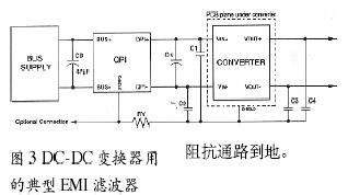
Compared with passive scheme, active filter can reduce the volume of common mode choke pattern and provide a low size surface mount device. In particular, the active EMI filter also reduces the size of the inductor, enabling the EMI filter to be packaged in a 110.2 inch package. The smaller size saves valuable board area, reduces height, and increases airflow in board applications, which helps board designers recover some of the lost space needed for EMI control. The active filter's 7A rating easily handles the current required for 200W ATCA boards.
The test results show that the active power filter is effective in reducing the total conducted noise below the required limit value.
Multifunctional input filter module
Some DC-DC converter vendors also offer AC-DC module front ends. This device has a variety of functions, including EMI filtering. For example, one such module is the filter/auto-regulating rectifier, which provides EMI filtering, auto-regulating line rectification, and starting current limiting. This allows designers to meet the EMI requirements of various standards.
EMI filter scheme for reducing input noise
The switched DC-DC converter also presents ripple and noise in its output. This output noise, often referred to as periodic and random Deviation (PARD), is the sum of the noise components on all ripple and superimposed power supply DC outputs. The ripple and noise levels of the switching DC-DC converter are tens of millivolts.
The output ripple attenuator module, which combines active and passive filtering functions, can limit output noise to less than 3mV peak-to-peak at loads up to 20A. Such a module is 2.282.40.5 inches in size and can attenuate the fundamental and harmonic waves of the low-frequency input power supply in the frequency range of DC~20MHz, with an efficiency of 93~99%.
Another output ripple attenuator in a single-package system (SiP) uses active filtering to reduce power output ripple and noise (PARD) by more than 30dB in the range of 1KHz to 500KHz. This structure improves transient response and ensures static load point adjustment. It adjusts the load using the remote sensing characteristics of the converter or the regulating pins of the device.
免责声明: 本文章转自其它平台,并不代表本站观点及立场。若有侵权或异议,请联系我们删除。谢谢! Disclaimer: This article is reproduced from other platforms and does not represent the views or positions of this website. If there is any infringement or objection, please contact us to delete it. thank you! |

WeChat Official Account

WeChat Service
 Email
Email QQ
QQ 13823761625
