
The need for green energy standards, lower costs and higher audio fidelity is driving the adoption of Class D amplifiers in high power audio. Traditional analog implementations, such as Class AB topologies, are complex and inefficient, but occupy the high-end audio market due to their high-fidelity performance for audio. Class D systems are designed to be simpler, more efficient, and offer high fidelity capabilities comparable to analog amplifiers, and are rapidly closing the gap in the high-end audio market.
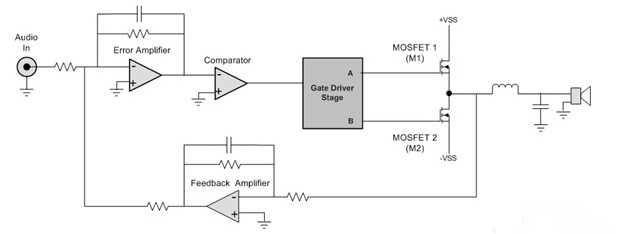
A typical Class D audio system first converts the analog audio input signal into a digital PWM signal, amplifies the power in the digital domain, and then converts the digital signal into an analog audio signal output. As shown in Figure 1, the input audio signal is sent to a pulse-width modulator (PWM) consisting of an operational amplifier and a comparator, which digitizes the audio by generating a modulated duty cycle signal proportional to the instantaneous value of the audio input signal.
Class D amplifier design
efficacy
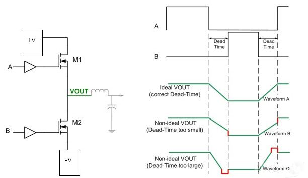
The traditional analog power amplifier depends on the linear amplifier circuit, which is easy to cause high power loss. In contrast, Class D amplifiers can achieve power efficiency of 90% or more (depending on the design). This benefit of high efficiency is inherent in Class D amplifier technology, where the amplification mechanism uses binary conversion (typically a power MOSFETs). These switches are either fully on or completely off, with very little time spent on state transitions. Discrete switching action and low MOSFET on-impedance reduce I2R losses and improve efficiency. In practice, however, the switching time (dead time) must be long enough to avoid a sharp drop in efficiency when two switches are running simultaneously.
High fidelity
Audio fidelity can be defined as the integrity of the sound after regeneration, and for audio systems, fidelity has always been synonymous with sound quality. Other metrics are also used to measure fidelity, some of which can be particularly challenging for designers to measure. The two most challenging metrics are: total harmonic distortion (THD) and noise (N), collectively known as THD+N.
THD is an accurate measurement of an audio system, very similar to hi-fi itself. The error of the regenerative signal comes from the input frequency harmonics generated by other components, which is clearly different from the pure output signal. THD is the ratio of all excess harmonic frequency energy to the basic input frequency energy, typically measured at half the power of a given system. THD performance is typically less than 0.1% for most non-hi-fi audio applications, and discerning listeners often require a THD rating as low as 0.05% or even lower.
The output noise level is a measurement of the background noise level of an amplifier output without signal input. For most speakers, the background noise of 100-500uV is not audible within normal listening distance, and the background noise of 1mV is too noisy, so THD+N is a good indicator of the audio fidelity of the amplifier.
Class D driver ics: Features and benefits
Programmable dead zone time
Class D amplifier dead time (i.e. the time period when both switches are off) directly affects efficiency and THD. Too short dead time will cause through current, reduce efficiency, and too long dead time will increase THD, which will adversely affect the audio fidelity.
Dead-time must be precisely set to find the "sweet spot" that optimizes both power efficiency and THD. Current typical high-voltage audio drivers have imprecise, overlapping dead-time Settings (i.e., 1/n delay values). Therefore, most designers choose to use discrete components to deal with dead time, which is not only expensive but also time-consuming. A simple and economical solution is to integrate a gate driver with a high-precision dead zone generator.
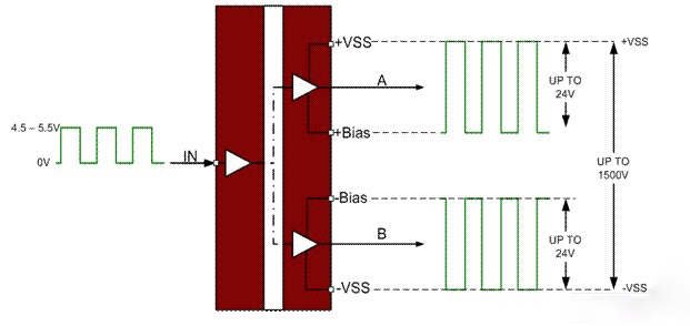
Due to the requirement of input level conversion, it may be difficult to implement two-state class D amplifiers. In high power Class D amplifiers, it is best to provide a high voltage supply rail (±VSS) for the power MOSFET stage. In practical Class D amplifier designs, a voltage of ±100Vdc can produce up to 600W of audio power on an 8Ω load.
Most existing high-voltage IC (HVIC) Class D drivers lack the ability to convert the low-voltage modulation portion into the high-voltage supply portion. Drivers that can provide level conversion have other shortcomings that make it difficult to be ideal for Class D operations (for example, the driver output ground terminal uses a negative voltage rail, requiring the input drive signal level to be converted to a negative power supply). Adding this capability through discrete devices is costly, difficult to design and takes up a lot of space, and level switching solutions with high-voltage bipolar supply interfaces are significant advantages of Class D designs.
In general, most drive solutions do not provide input/output isolation, nor isolation between drives, so additional elements are required to provide level switching mechanisms.
High-frequency operation
One of the best features of Class D gate drivers is the ability to operate at high switching frequencies with minimal propagation delay. These characteristics make the total loop delay on the feedback path very low, achieving the best possible noise performance. Operating at higher frequencies also improves the "cycle gain" and improves the distortion performance of the amplifier. Most existing HVIC drivers only support modulation frequencies up to 1MHz.
Integration degree
In today's competitive global market, a solution that integrates all of these features will be a great convenience for Class D amplifier designers, who can bring their products to market earlier by reducing design time, reducing the number of components, reducing insertion costs, and lower reliability due to the larger number of devices.
Brief summary
Class D amplifiers have features that go far beyond traditional analog amplifiers, including lower THD, smaller board space, higher power efficiency, and lower BOM costs. Highly integrated gate driver ics have a significant positive effect on both system architecture and audio performance. Silicon Labs' Si8241/8244 audio driver is the first high-power Class D amplifier solution to integrate all features into a single IC package. The benefits of these gate drivers include: high-precision dead-time Settings for minimum THD and optimal power performance; No need to add complex design and number of devices for input signal level conversion; Isolated output driver, simplify the implementation of two-state switch; It has high inhibition to transient power supply.
免责声明: 本文章转自其它平台,并不代表本站观点及立场。若有侵权或异议,请联系我们删除。谢谢! Disclaimer: This article is reproduced from other platforms and does not represent the views or positions of this website. If there is any infringement or objection, please contact us to delete it. thank you! |

WeChat Official Account

WeChat Service
 Email
Email QQ
QQ 13823761625
