People often take it for granted to power the circuit of the PCB, not knowing that this can cause damage and damage or non-destructive latch conditions. These problems may not be prominent until the start of mass production, when the tolerance of the device and design is tested, but it is too late, the project and product time and delivery will be greatly affected, and the cost will be greatly increased. To address the errors found during this phase, a number of modifications will be required, including PCB layout changes, design changes, and additional anomalies.
With the advent of the integrated circuit era, many functional modules are integrated into one IC, so it is necessary to use multiple power supplies to power these modules. The voltages of these sources are sometimes the same, but more often they are different. The increasing number of system-on-chip (SoC) ics on the market has created a need for sequential control and management of power supplies.
Analog Devices' data books usually provide enough information to guide design engineers in designing the correct power-on sequence for each IC. However, some ics explicitly require that an appropriate power-on sequence be defined. This is true for many of Analog Devices' ics. This requirement is common in ics that use multiple power supplies, such as converters (including ADC and DAC), digital signal processors (DSPS), audio/video, RF, and many other mixed-signal ics. Essentially, ics that contain some kind of analog input/output with a digital engine fall into this category and may require specific power timing control. These ics may have separate analog and digital power supplies, and some even have digital input/output power supplies, see the specific examples discussed below for details.
This application note discusses some of the more subtle power supply issues that design engineers must consider in a new design, especially when the IC requires multiple different power supplies. At present, some of the more commonly used power supply voltages are: +1.8V, +2.0V, +2.5V, +3.3V, +5V, +12V, and −12V.
PULSAR ADC example - Absolute maximum rating
All Analog Devices data books contain an Absolute Maximum Rating (AMR) section, which describes the maximum voltage, current, or temperature that can be applied to the pin or device to avoid causing damage.
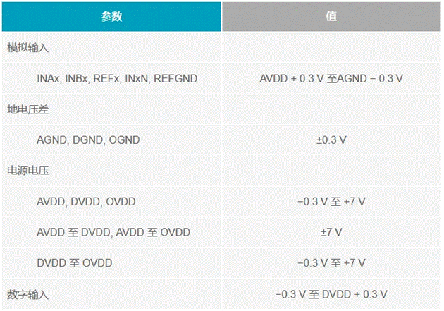
The AD7654PulSAR 16-bit ADC is an example of a mixed-signal ADC with three (or more) independent power supplies. These ADCs require a digital power supply (DVDD), analog power supply (AVDD), and digital input/output power supply (OVDD). They are ADCs that convert analog signals into digital code, so an analog core is required to process the incoming analog input. The digital kernel handles the bit determination process and control logic. The I/O kernel is used to set the level of the digital output for interface with the host logic (level conversion). The power supply specifications for the ADC can be found in the "Absolute Maximum Rating" section of the corresponding data sheet. Table 1 is taken from the "Absolute Maximum Ratings" section of the AD7654 (Rev.B) data book.

Similarly, the digital input voltage ranges from −0.3V to DVDD +0.3V. This means that the digital input must be less than DVDD +0.3V. Therefore, when powering on, the DVDD must be powered on before or at the same time as the microprocessor/logic interface circuit. Similar to the analog core situation described above, ESD diodes on these pins can also become positively biased, powering the digital core to an unknown state.
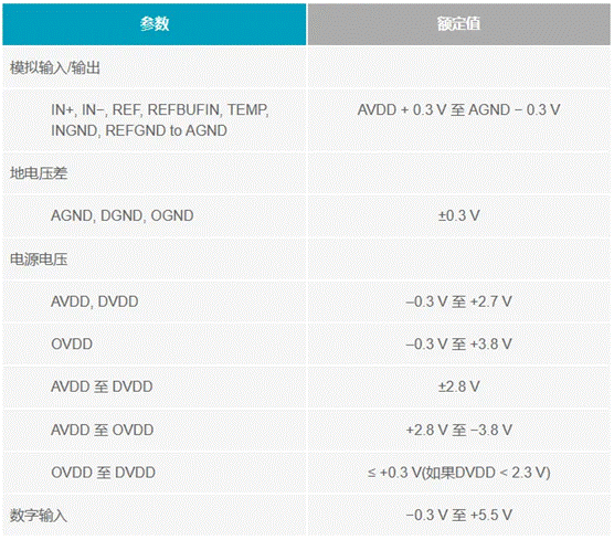
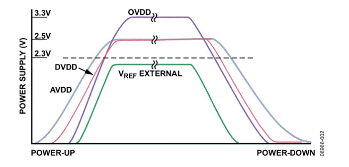
PulSAR ADCs such as the AD7621, AD7622, AD7623, AD7641, and AD7643 are newer to the family and use a lower 2.5V power supply (the AD7654 uses a 5V power supply). The AD7621 and AD7623 have a well-defined power-on sequence. Table 2 is taken from the "Absolute Maximum Ratings" section of the AD7621 (Rev.0) data book.


Example of type Σ-Δ ADC
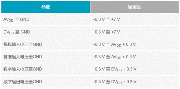
AD7794 type Σ-Δ 24-bit ADC is another good example. Table 3 is taken from the "Absolute Maximum Ratings" section of the AD7794 (Rev.D) data book.

Power sequential controller
Analog Devices offers a number of power sequential control devices. In general, the working principle is that when the output voltage of the first regulator reaches a preset threshold, a time delay is initiated, and subsequent regulators are powered on only after the delay is over. The procedure during a shutdown is similar. A timing controller can also be used to control the timing of logical signals such as power supply good signals, for example by applying a reset signal to a device or microprocessor, or simply indicating that all power supplies are active.
Suggestion
Today, most circuit PCBS that require high speed and low power consumption require multiple power supplies, such as +1.8V, +2.0V, +2.5V, +3.3V, +5V, +12V, and −12V. Powering these power supplies on a PCB is no easy task. Careful analysis is required to design a correct and reliable power-on and shutdown sequence. The use of discrete design is becoming more and more difficult, the solution is to use the power timing control IC, as long as a change in the code can change the power-on sequence, without changing the PCB layout.
免责声明: 本文章转自其它平台,并不代表本站观点及立场。若有侵权或异议,请联系我们删除。谢谢! Disclaimer: This article is reproduced from other platforms and does not represent the views or positions of this website. If there is any infringement or objection, please contact us to delete it. thank you! |


