By Remy Zhang
This document introduces the typical design of Class D audio power amplifier, Outlines the basic applications of gallium nitride devices in Class D audio power amplifier, and briefly introduces the advantages of gallium nitride devices in Class D audio power amplifier design compared to silicon devices.
A typical design of a Class D audio amplifier
1.1. What is a Class D audio power amplifier?
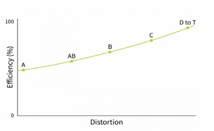
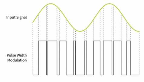
The Class D amplifier was first invented by British scientist Alec Reeves in 1950. In simple terms, a Class D power amplifier is an electronic amplifier, also known as a power switching amplifier, operating on pulse width modulation, which converts the input signal into a pulse stream. The output transistor stage of a Class D power amplifier operates as an electronic switch and does not have the linear gain of other amplifiers. A Class D power amplifier starts by receiving the incoming analog input signal and generating PWM or PDM. It then converts the input signal into a stream of pulses. Therefore, it can be said that a typical Class D power amplifier consists of two output MOSFETs, a pulse width modulator, and an external low-pass filter to recover amplified audio.
1.2. The working principle of Class D audio amplifier
Class D amplifiers produce a series of rectangular pulses of fixed amplitude at the beginning of operation, varying in area and interval, or number per unit time. In addition, the amplitude change of the analog audio input stream is also represented by these pulses, and it is also feasible to synchronize the modulator clock with the input digital audio input signal, so there is no need to convert the digital audio signal to analog. The output stage of the modulator controls their operation by alternately turning the output transistors on and off.
Advantages of gallium nitride devices in Class D audio amplifier applications
To start with, the advantages of gallium nitride switching devices compared to silicon-based transistors used in Class D audio amplifiers are mainly the following three points:
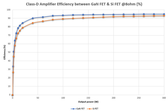
Higher overall efficiency
The distortion index has improved
The switching waveform is clearer so how does the gallium nitride switching device bring the above three advantages to the Class D audio amplifier?
2.1. Higher overall efficiency
First of all, in order to achieve the excellent performance of Class D audio amplifiers, it is necessary to provide the lowest possible on-resistance to minimize on-loss. GaN switching devices provide much lower on-resistance than silicon-based transistors and achieve this over a much smaller bare chip area.
Secondly, switching loss is another factor that needs to be considered. At medium to high power output, Class D amplifiers are extremely efficient. However, when it is in a low power output state, the efficiency is much lower than the medium and high power output due to the loss in the power device.
To overcome this challenge, some Class D amplifiers use two modes of operation. Once the output power level reaches a predetermined threshold, the output voltage rail of the power amplifier switch tube is raised to provide a full scale voltage swing. Therefore, in order to further reduce the impact of switching losses, zero voltage switching (ZVS) technology can be used at low output power levels, and hard switching can be changed at high power levels, and the extremely low switching loss at zero voltage switching (ZVS) state of gallium nitride devices can be used to improve the overall efficiency of the system at low output power.
2.2. The distortion index has improved
hen the Class D audio amplifier is operated in ZVS mode, the switching loss is effectively eliminated, because the output conversion is achieved by inductive current reversal. However, like all other half-bridge designs, we need to take into account the straight-through problem, that is, the moment when the high-side and low-side switches are on simultaneously. We usually insert a short delay called Blanking time to ensure that one of the switching tubes is fully closed before the other switches on.
is important to note that this delay affects the PWM signal and causes distortion in the audio output, so the goal is to make it as short as possible to maintain the fidelity of the audio. The length of this delay mainly depends on the output capacitance Coss of the power device, and although GaN transistors have not completely eliminated Coss, it is significantly lower than that of silicon-based switching devices. Therefore, the shorter blanking time allows Class D audio amplifiers to have less distortion when GaN is used as a switching device. In the field of professional speakers, the subtle THD gap can bring a completely different hearing experience to consumers.
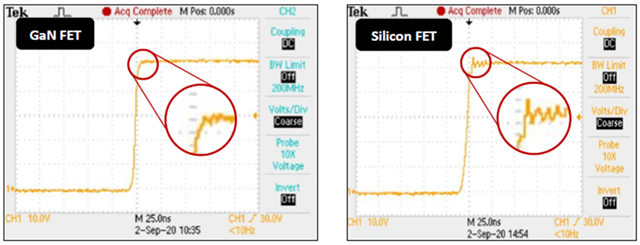
As with any audio amplifier, an important indicator of the performance of any Class D audio amplifier is the degree of reproduction of the audio signal, and for "switching amplifier" systems, such as Class D audio amplifiers, one of the main goals is to use the "perfect" switching waveform. The closer the switching waveform is to "perfect," the closer the audio reproduction will be to "perfect."
When silicon based transistors are used to implement switching functions in Class D audio amplifiers, hard switching mode causes charge accumulation in the body diode because the voltage at the output is not zero when the power device is turned off and on, and then the established reverse recovery charge (Qrr) needs to be discharged. The discharge time needs to be taken into account in the PWM control action. In designs using GaN, this is no longer an issue, because GaN transistors do not have the bulk diodes inherent in silicon-based transistors, so there is no reverse recovery charge Qrr, allowing us to get a clearer switching waveform.
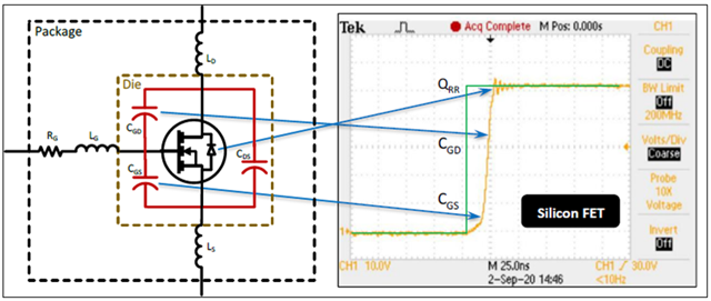
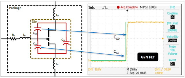
It can be clearly seen from the figure above that reverse recovery charge (Qrr), Cgs and Cgd have a serious negative impact on the restoration of the switching waveform of silicon-based switching devices. However, due to the absence of reverse recovery charge (Qrr) in GaN switching devices and the very low Cgs and Cgd, The negative effects of such charge parameters are very limited.
Three summaries
For many years, silicon-based switching devices have served designers of Class D audio amplifiers well, thanks to continuous advances in optimizing their performance. However, it is challenging to make further improvements in their characteristics. In addition, further reductions in on-resistance RDS(on) result in larger chip sizes, making it more difficult to build compact audio amplifier designs. However, GaN switching devices break through this limitation while also eliminating Qrr, which, combined with their Coss reduction and ability to operate at higher switching frequencies, means that smaller, more compact designs can be easily built. The resulting THD+N measurements also indicate that this new technology can achieve superior audio performance.
免责声明: 本文章转自其它平台,并不代表本站观点及立场。若有侵权或异议,请联系我们删除。谢谢! Disclaimer: This article is reproduced from other platforms and does not represent the views or positions of this website. If there is any infringement or objection, please contact us to delete it. thank you! |


