1 Introduction
In recent years, as the input voltage requirements of computer microprocessors are getting lower and lower, the study of low-voltage and high-current DC-DC converter has been paid more and more attention by many researchers. Various topologies are emerging in an endless stream, and synchronous rectification technology, multiple polyphase technology, magnetic integration technology and so on are also applied in this field. In this paper, a staggered parallel low-voltage and high-current DC-DC converter is proposed. The primary side adopts a symmetrical half-bridge structure, while the secondary side adopts a double-current rectifier structure. This structure can greatly reduce the current ripple on the filter capacitor, thus greatly reducing the size of the filter inductor and the size of the whole DC-DC converter. The converter operates in an environment of 48V input voltage and 100kHz switching frequency.
Structure analysis of low voltage high current DC-DC converter with double current rectification
The circuit principle diagram of low-voltage and high-current DC-DC converter is shown in Figure 1. The symmetrical half-bridge structure is adopted on the primary side, and the double-current rectifier structure is adopted on the secondary side. When S1 is on, SR1 must be cut off and L1 is charged. SR2 must be cut off and L2 charged when S2 is switched on, so that the filter inductor current will be superimposed on the filter capacitor. Figure 2 shows the switching control strategy.
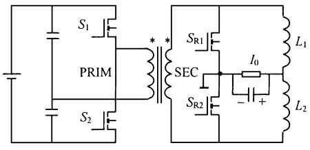
FIG. Circuit schematic diagram of low voltage high current DC-DC converter with 1 times current rectification
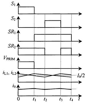
Through the above analysis, it can be seen that the two filtering inductance currents on the secondary side of the double-current rectifier structure are superimposed on each other on the filtering capacitor, so that the output current ripple becomes quite small.
The synchronous rectifier in the structure is driven by an external signal, which makes the control very complicated. However, it is difficult to use a simple self-drive method in this half-bridge-current topology, because in this structure, if the appropriate point is directly taken from the circuit as the driver signal of the synchronous rectifier, when the driver signal is zero in the dead zone time, the control system will be improved. The synchronous rectifier will cut off. In order to use the self-drive mode in the half-bridge-multiplier topology, auxiliary windings must be used.
Taking a single half-bridge and current-doubling topology as an example, see Figure 3, where VSEC is the secondary side voltage of the transformer and Vgs is the drive voltage of the synchronous rectifier obtained by the auxiliary winding. It can be seen that the drive voltage of the synchronous rectifier cannot be zero even within the dead time, which ensures the application of self-drive mode in this topology.
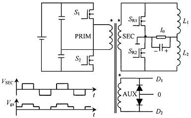
Figure 3 Self-driven synchronous rectifier circuit and waveform diagram
In addition, because the on-voltage drop of MOSFET will increase in the case of high current, resulting in large on-loss, multiple MOSFETs should be used in parallel to reduce the loss.
3 Staggered parallel low voltage high current DC-DC converter
3.1 Schematic diagram of circuit
To sum up, the double-current-rectified low-voltage high-current DC-DC converter has good performance. On this basis, a new structure called the parallel low-voltage high-current DC-DC converter is formed by introducing the interleaved parallel parallel technology, which can further reduce the output current ripple.
e 4 shows the circuit schematic diagram of the interleaved parallel low-voltage and high-current DC-DC converter (taking the simplest two-fold commutation interleaved parallel as an example).
Figure 4 Circuit schematic diagram of interleaved parallel low-voltage high-current DC-DC converter
3.2 Switching control strategy of converter
The switching control strategy of the interleaved parallel low-voltage high-current DC-DC converter is shown in Figure 5.
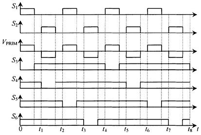
3.3 Performance of staggered parallel low-voltage and high-current DC-DC converter
First of all, the biggest advantage of this topology is that the structure of the original side of the transformer is simplified, and the control is very simple. Secondly, the realization of this method must use a synchronous rectifier circuit, because the realization of the staggered parallel circuit requires that the transformer sub-side and lower potentials take turns to be positive, and only one is positive in a period of time, and the rest are zero potential. However, in this topology, because the primary sides of the two transformers are connected in series, and the secondary sides are in parallel, so if the Schottky diode is used as the rectifier, then the input voltage will be divided on the original sides of the two transformers, and the Schottky diode has no gate function, so that the waveform on the secondary side of the transformer will be completely symmetric, and the current of the upper and lower two rectifier circuits will be completely coexisting. Can not achieve the purpose of current interleaving parallel.
In this way, the synchronous rectifier is used to accomplish this function, while taking advantage of the bidirectional conductive characteristics of the MOSFET, because the drain-source current of the synchronous rectifier is distributed on both sides of the coordinate horizontal axis. The process of this structure is analyzed in detail as follows:
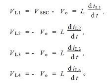
1) S1 is on, S2 is off; S3 is off, S4, S5, and S6 are all connected. Due to the turn-on of S4, S5, S6, the lower end of the first transformer's secondary winding is zero potential, the upper and lower ends of the second transformer's secondary winding are zero potential, the current on the inductor L1 rises, and the current on L2, L3, L4 drops.
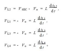
2) S2 is on, S1 is off; S4 is off, S3, S5, and S6 are all connected. Due to the on-going of S3, S5 and S6, the upper end of the secondary winding of the first transformer is zero potential, and the upper and lower ends of the secondary winding of the second transformer are zero potential, and the current on the inductor L2 is increased, and the current on L1, L3 and L4 is decreased.
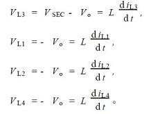
3) S1 is on, S2 is off; S5 is off, S3, S4, and S6 are all connected. Due to the on-going of S3, S4, S6, the lower end of the secondary winding of the second transformer is zero potential, the upper and lower ends of the first transformer are zero potential, the current on the inductor L3 rises, and the current on L1, L2, L4 drops.
4) S2 is on, S1 is off; S6 is off, S3, S4, and S5 are all connected. Due to the on-going of S3, S4, S5, the upper end of the secondary winding of the second transformer is zero potential, the upper and lower ends of the first transformer are zero potential, the current on the inductor L4 rises, and the current on L1, L2, L3 drops.
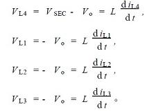
All the above types ignore the voltage drop of the rectifier, and VSEC is the voltage value of the secondary side of the transformer.
ccording to the above analysis, the staggered parallel half-bridge-current multiplier topology can be realized by using synchronous rectifier and connecting the primary side of transformer in series and the secondary side in parallel. Its advantages mainly have the following aspects:
1) The topology structure and control strategy are effectively simplified.
2) In the case of constant frequency, if the peak-to-peak value of the ripple is certain, this structure can effectively reduce the value of the filter inductor, thereby speeding up the dynamic response time of the entire converter.
3) Compared with the non-interleaved half-bridge-current-doubling topology, the on-loss of the primary side and the secondary side is similar, but due to the use of interleaved parallel technology, the switching frequency of the secondary side is half of the original, and the corresponding switching loss is also half of the original. Because the switching loss of the converter accounts for a large proportion in the whole loss statistics, the interleaving and parallel technology can greatly improve the efficiency of the converter.
4 Simulation Analysis
Pspice software is used to simulate the circuit. The circuit parameters are as follows: the switching frequency is 100kHz, the duty cycle is 40%, the input voltage is 48V, the filter inductance is 2μH, the filter capacitance is 820μF, the output current is 60A, and the output voltage is 1125V.
FiG. 6 shows the current waveform of the filtered inductors. It can be seen from FIG. 6 that the currents of the four filtered inductors are charged in turn. If one filtered inductor is charging, the other three inductors must discharge.
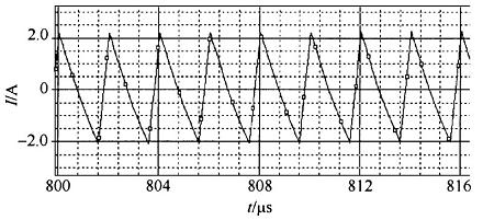
FIG. 7 and FIG. 8 show the output current ripple shapes of the interleaved parallel converter and a single double-commutator, respectively. It can be seen from FIG. 7 that the current of four filter inductors superimposed on the filter capacitor can greatly reduce the current ripple.
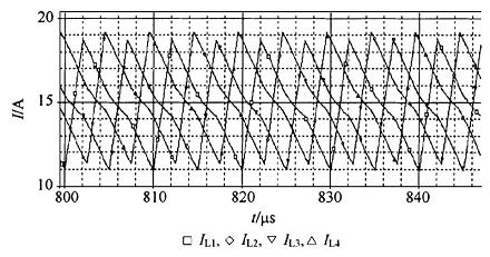
FIG. 6 Waveform of filtered inductance current
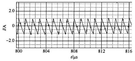
Figure 7 Output current ripple shape of staggered parallel converter structure
5 Experimental Results
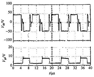
Through theoretical research and simulation analysis, it can be seen that the staggered parallel low-voltage high-current DC-DC converter has good performance, and the output current ripple can be reduced to a small size when the output is 1125V/60A. In order to further illustrate the feasibility of this topology structure, experimental results are used to verify it. The experimental circuit is shown in Figure 4, and the experimental parameters are the same as those of the simulation. Finally, the experimental waveform as shown in Figure 9 is obtained. In FIG. 9, Vgs is the gate drive voltage waveform of a primary MOSFET, and Vds is the gate-source voltage waveform of the corresponding MOSFET. As can be seen from FIG. 9, the waveform obtained from the experimental results is in good agreement with the theoretical analysis results in FIG. 5, and the proposed method is feasible. Among them, GU22 core made of R2KB soft magnetic ferrite material is selected for the transformer, and the number of turns of the primary side is 8 turns and 1 turn, respectively. The inductance is made of ring core T5-10 215 made of wide constant permeability magnetic material IJ50h, with 8 turns.
6 Concluding Remarks
Through simulation and experimental analysis, the following conclusions are drawn: for low-voltage and high-current DC-DC converter, the output current ripple can be further reduced by interlacing and parallel, and the effect is very obvious; Or in the case of the same output current ripple, the filter inductance value can be greatly reduced, thus reducing the size of the whole converter and improving the transient response characteristics of the converter. The two cases discussed in this paper are also suitable for the case of multiple multiple structures.
免责声明: 本文章转自其它平台,并不代表本站观点及立场。若有侵权或异议,请联系我们删除。谢谢! Disclaimer: This article is reproduced from other platforms and does not represent the views or positions of this website. If there is any infringement or objection, please contact us to delete it. thank you! |


