
Source: ON Semiconductor
On the roads, the number of vehicles powered by batteries is increasing day by day. In the home, all kinds of devices, from handheld power tools to lawn mowers, have been made wireless. In the construction field, equipment such as hammer drills, impact wrenches, circular saws, and nail guns are also powered by batteries. In the warehouse, material handling equipment such as forklifts, pallet trucks, and automated guided vehicles (AGVs) have all benefited greatly from the improvement in battery performance.

As battery-powered devices become increasingly popular, fast charging is crucial for enhancing the convenience of such devices. This article discusses the standards that must be considered when designing an efficient battery charging system, introduces the more commonly used topologies, and elaborates on how onsemi's power semiconductors can help achieve high-performance solutions.
Battery charging system
The battery charging system is suitable for various types of chemical batteries, including lead-acid batteries, nickel-metal-hydride batteries and lithium-ion batteries. At present, most battery-powered devices use 12V to 120V lithium-ion or lithium phosphate batteries. Battery chargers must be designed according to the requirements of the application and the working environment. For handheld power tools, the battery charger must be compact, lightweight and capable of operating without forced heat dissipation. Such small and highly efficient chargers require high energy density, which demands that the chargers must have low power loss and smaller heat sinks, while fast charging requires high-frequency chargers.
In industrial applications, chargers must be robust and durable, capable of withstanding harsh indoor and outdoor environments, and may require power supply from 120-277V AC power, or even 480V AC power.
Therefore, designers must carefully select the best topology for their final application and optimize the device selection to meet the cost-performance requirements.
Battery charging topology
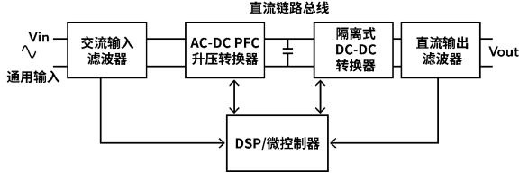
Figure 1 shows the block diagram of a typical battery charging system. At the front end, the input voltage from the mains power supply is filtered and then converted into DC voltage through a power factor correction (PFC) circuit. The second stage of this system consists of DC-DC conversion and constant voltage/constant current control functions, which are used to provide the required charging output.
Select the best topology for the application
Next, we will analyze several circuit topologies and discuss their applicability in different battery-powered applications.
1. PFC topology
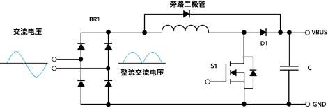
The continuous conduction mode boost topology (Figure 2) is the simplest and lowest-cost PFC topology, which consists of an input EMI filter, a bridge rectifier, a boost inductor, a boost FET and a boost diode.
For higher-power applications, ON Semiconductor's FAN9672 and FAN9673 PFC controllers are good choices. Silicon carbide (SiC) has significant advantages in charging applications, including low switching losses and high operating frequencies. Therefore, it is recommended to use SiC boost diodes in PFC design. In high-power applications ranging from 2KW to 6.6KW, the loss of the input bridge is significantly higher. By replacing diodes with active switches such as Si MOSFETs or SiC MOSFETs, these losses can be reduced.
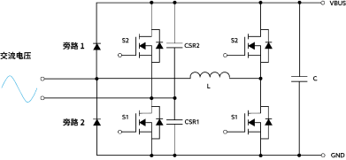
Other common topologies include semi-bridge-free PFC and totem-pole PFC (TPFC), which eliminate bridge rectifiers and have lower losses. The TPFC (Figure 3) consists of an EMI filter, a boost inductor, a high-frequency half-bridge, a low-frequency half-bridge, a dual-channel gate driver and a fixed-frequency TPFC controller.
On Semiconductor's 650V EliteSiC MOSFET offers a range of options for high-frequency bridge arms designed for TPFC. For 3.0kW applications, NTH4L032N65M3S can be considered. For applications up to 6.6kW, NTH4L015N65M2 and NTH4L023N065M3S are good choices. For the low-frequency bridge arm of the TPFC circuit, the NTHL017N60S5 device is a suitable choice.
2. Isolated DC-DC converter
For isolated DC-DC conversion, a variety of different topologies can be adopted depending on the power level of the application.
The half-bridge LLC topology with a secondary-side synchronous bridge rectifier (Figure 4) is highly suitable for charger applications ranging from 600W to 3.0KW. Depending on the power level, GAN power switches (NCP58921, 600W to 1.0KW) or SiC MOSFETs (2KW and 3.0KW) can be used. For applications with higher power levels (4.0KW to 6.6KW), designers should consider using full-bridge LLC (Figure 5) or interlaced LLC topology.
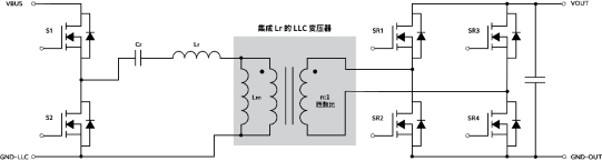

Figure 5: Full-bridge LLC topology with secondary voltage multiplier circuit
Applications such as ride-on lawn mowers, forklifts and electric bicycles may require dual active bridge (DAB) charging solutions with power levels ranging from 6.6KW to 11.0KW. The dual active bridge topology (Figure 6) is suitable for applications ranging from 6.0KW to 30.0KW, and multiple 6.0KW chargers can be used in parallel to support applications from 12.0KW to 30KW.

图 6:双有源桥技术

On Semiconductor's product portfolio includes 650-750V Elite SiC MOSFETs and iGaN HEMT devices suitable for bidirectional switching applications. The NTBL032N65M3S and NTBL023N65M3S EliteSiC MOSFETs are recommended for primary bidirectional switching and are also applicable to iGaN technology.
Optimize topology and device selection
The convenience of power tools and equipment depends on whether the battery can be charged quickly and efficiently. Designers of battery charging solutions must take into account the required power level and operating voltage, and carefully select the best topology. In addition, the devices selected by the designers for the design must be able to meet the performance requirements of the application.
On Semiconductor's product portfolio covers a wide range of low-voltage, medium-voltage and high-voltage power discrete devices, including silicon-based devices such as diodes, MOSFETs and IGBTs. Sic-based switching devices are increasingly favored because they offer faster switching speeds and excellent low-loss operating characteristics, enabling them to increase power density without sacrificing performance. With ON Semiconductor's chip and packaging technologies, ON Semiconductor's power devices feature outstanding quality and robustness, enabling you to exceed your design goals.
免责声明: 本文章转自其它平台,并不代表本站观点及立场。若有侵权或异议,请联系我们删除。谢谢! Disclaimer: This article is reproduced from other platforms and does not represent the views or positions of this website. If there is any infringement or objection, please contact us to delete it. thank you! |

WeChat Official Account

WeChat Service
 Email
Email QQ
QQ 13823761625
