Products
Products
PED2313N DFN2x3-6L
PED2313N is VDS=18V, ID=9.5A, RDS(ON)<9mΩ@VGS=4.5V, RDS(ON)<10mΩ@VGS=3.8V, RDS(ON)<11.5mΩ@VGS=3.1V, An n-channel MOSFET with RDS(ON)<14 Mω@vGS =2.5V.
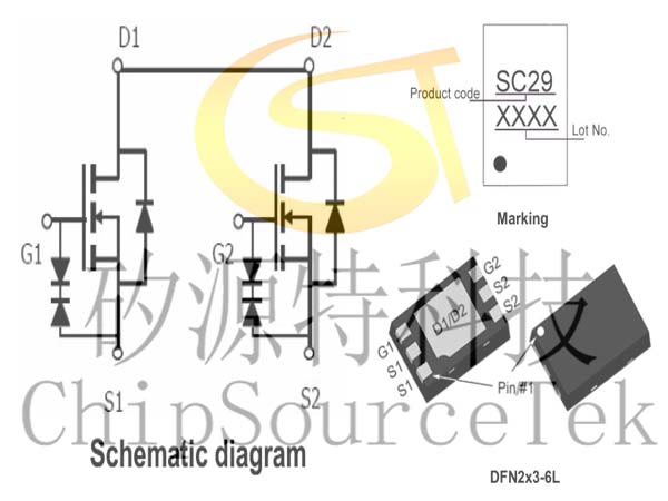
The screen printing of PED2313N is SC29.
PED2313N is available in DFN2x3-6L package.
The PED2313N uses advanced trench technology to provide excellent RDS(ON) and low gate charge. It can be used in a wide variety of applications. It is ESD protected.
The screen printing of PED2313N is SC29.
PED2313N is available in DFN2x3-6L package.
The PED2313N uses advanced trench technology to provide excellent RDS(ON) and low gate charge. It can be used in a wide variety of applications. It is ESD protected.
PED2313N Description:
PED2313N is VDS=18V, ID=9.5A, RDS(ON)<9mΩ@VGS=4.5V, RDS(ON)<10mΩ@VGS=3.8V, RDS(ON)<11.5mΩ@VGS=3.1V, An n-channel MOSFET with RDS(ON)<14 Mω@vGS =2.5V.
The screen printing of PED2313N is SC29.
PED2313N is available in DFN2x3-6L package.
The screen printing of PED2313N is SC29.
PED2313N is available in DFN2x3-6L package.
The PED2313N uses advanced trench technology to provide excellent RDS(ON) and low gate charge. It can be used in a wide variety of applications. It is ESD protected.
PED2313N Features:
VDS = 18V, ID = 9.5A
RDS(ON) < 9mΩ @ VGS=4.5V
RDS(ON) < 10mΩ @VGS=3.8V
RDS(ON) < 11.5mΩ @VGS=3.1V
RDS(ON) < 14mΩ @VGS=2.5V
ESD Rating: 4000V HBM
High Power and current handing capability
Lead free product is acquired
Surface Mount Package
PED2313N Application:
PWM applications
Load switch
Power management
PED2313N Typical application and pin:


