
Products
Products


TR16F900B
The TxP16ETM is a high-performance 16-bit MCU operating at up to 32MHz with 64K FLASH and 4K SRAM for high-performance processing of speech recognition algorithms, power control and motor control. It is a new generation computing kernel of Flash DSP series. It was originally targeted at controllers and multimedia digital signal processing (DSP) applications to demonstrate its expertise. The TxP16E provides a fast MAC architecture that allows multiply + add instructions to be issued simultaneously to the access memory in one cycle. The TR16F900 is equipped with a TxP16E and integrated input/output port, audio PWM, timer and low voltage reset. Let's wait.
In addition, the TR16F900 extends its ability to connect external devices, such as serial ROM/Flash. Internal memory capacity includes 64Kx16 program/data FLASH and 4Kx16 working SRAM.
In addition, the TR16F900 extends its ability to connect external devices, such as serial ROM/Flash. Internal memory capacity includes 64Kx16 program/data FLASH and 4Kx16 working SRAM.
TR16F900B General Description:
The TxP16ETM is a high-performance 16-bit MCU operating at up to 32MHz with 64K FLASH and 4K SRAM for high-performance processing of speech recognition algorithms, power control and motor control. It is a new generation computing kernel of Flash DSP series. It was originally targeted at controllers and multimedia digital signal processing (DSP) applications to demonstrate its expertise. The TxP16E provides a fast MAC architecture that allows multiply + add instructions to be issued simultaneously to the access memory in one cycle. The TR16F900 is equipped with a TxP16E and integrated input/output port, audio PWM, timer and low voltage reset. Let's wait.
In addition, the TR16F900 extends its ability to connect external devices, such as serial ROM/Flash. Internal memory capacity includes 64Kx16 program/data FLASH and 4Kx16 working SRAM.
In addition, the TR16F900 extends its ability to connect external devices, such as serial ROM/Flash. Internal memory capacity includes 64Kx16 program/data FLASH and 4Kx16 working SRAM.
TR16F900B Features:
* Speech recognition
* High-performance RISC TxP16E CPU
- Wide operating frequency, voltage 1Mhz~32mhz@1.8volt~5.5 volts
- For flash erase and programming operations, the LVR needs to be set to equal or greater than 2.0V.
- The operating frequency can be programmed by software
- Built-in 4096x16 SRAM
- Mixed instruction and data memory shared with 64Kx16 flash ROM
- Embedded PC stack level 24
* Rich DSP features
- Hardware ring buffer support
-MAC Computing capability: up to 32MIPS
- Multi-function support: In MAC computing, access two operands in memory at the same time in one cycle
- Extended dynamic range: a 40-bit accumulator that ensures no overflow in 512 consecutive + addition operations
* Embedded flash 64Kx16
- Typical 20000 erase/programming cycles
- Data retention period of more than 10 years
* Software-based audio processing technology
- Sub-band, ADPCM, CELP, melody synthesis, up to 20 channels (Max)
* Supports 20+2 (ICE PAD can be used as I/O) universal I/O port, can be configured to open leakage output
* Stereo 8-16 bit PWM adjustable
*15 IRQ and 1 NMI
-NMI is an unmasked interrupt that interrupts IRQ immediately
-2 External interruption
* 4-bit SPI main hardware supports DMA transmission
*SPI Slaver
* Green mode
*Timer1, Timer2 with pre-scale
* Low power command
*24 hours/day real-time clock
*ICE supports data RAM monitors for motor control debugging
* Support spread spectrum timing to reduce EMI.
* Watchdog Timer (WDT)
* Low Voltage reset (LVR)
* Low Voltage Difference Regulator (LDO) Power supply 3.3V/1.8v@20ma (voltage drop 0.1v)
*PB0, PB1, PB2, and PB3 support two edge modes: rising edge trigger and falling edge trigger for wake-up function.
comparator
*ADC 10-bit /285 kbps (@ACQT=4*TAD) /8 channels
* Temperature. sensor
* Microphone
*1402 port
* For ACALL's new instructions, see "TxP16E Instruction Set Reference"
* For new instructions for 3OP, see "TxP16E Instruction Set Reference"
* For new instructions on barrel shifters, see "TxP16E Instruction Set Reference"
* For new instructions on immediate value CBL, see "TxP16E Instruction Set Reference"
* For notes on Flash DSP programming, see "Flash DSP Programming Notes (AN0060)"
TR16F900B Application Area: Test"
* Speech recognition
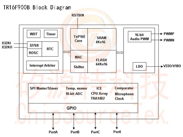
TR16F900B block diagram:
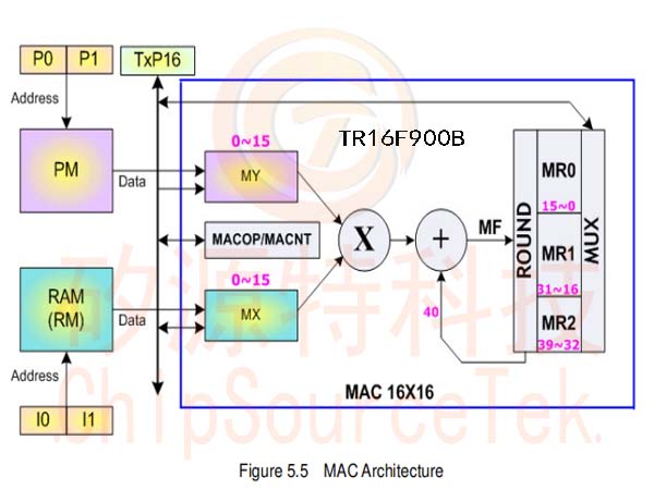
TR16F900B MAC (16-bit X 16-bit multiplier and accumulator) :
A 16-bit x 16-bit MAC is provided for digital signal processing. The core of the MAC operation is to multiply the complement operands of MX and MY by 2 and accumulate the previous 40-bit MF, then round off to store the result in the 40-bit Mr Register. The basic MAC architecture is shown in Figure 5.5.
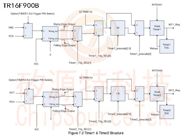
TR16F900B Timer 1 and Timer 2 Structure:
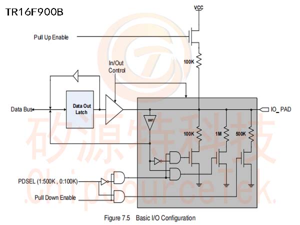
TR16F900B Basic I/O configuration:
TR16F900B high-speed 8-channel / 10-bit ADC structure diagram:
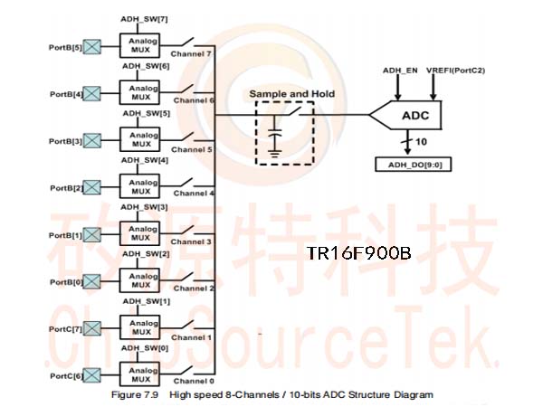
Note: If the user needs a more precise ADC for application, the user can set the "ADC vref input" to enable the VREFI option. If the ADC Verf input is enabled, the PortC2 must connect a 20~100 ohm resistor to the VCC and a 47uF capacitor to the AVSS. Otherwise, the IC will not work properly.
Note: Optionally enable the ADC verf input with PortC2 as the ADC voltage reference input (VREFI) instead of the I/O pin.
** Decoupling capacitors (10uF) must be as close to VCC and VSS as possible.
Note: Optionally enable the ADC verf input with PortC2 as the ADC voltage reference input (VREFI) instead of the I/O pin.
** Decoupling capacitors (10uF) must be as close to VCC and VSS as possible.
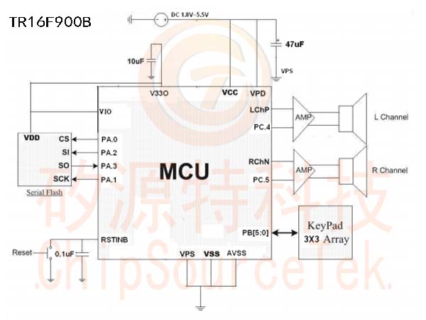
TR16F900B Application Circuit:
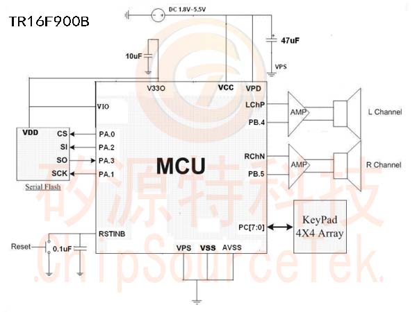
Application Circuit 1: Stereo 16-bit PWM AMP output with serial flash memory (TYPE1)
Attention:
1.VPD VPS decoupling cap 47uF, approach IC.
2. The power path of the VPD and VPS must enter the IC through the decoupling cap 47uF.
3.VCC VSS decoupling capacitor 0.1uF, please approach IC.
4. The power supply path of VCC and VSS must enter the IC through the decoupling cap 0.1uF.
5.VSS and AVSS are as close as possible.
6. For PCB layout of power cord, please refer to "Application Note (AN0059)"
Application Circuit 2: Stereo 16-bit PWM AMP output with serial flash memory (TYPE2)
Attention:
1.VPD VPS decoupling cap 47uF, approach IC.
2. The power path of the VPD and VPS must enter the IC through the decoupling cap 47uF.
3.VCC VSS decoupling capacitor 0.1uF, please approach IC.
4. The power supply path of VCC and VSS must enter the IC through the decoupling cap 0.1uF.
5.VSS and AVSS are as close as possible.
6. For PCB layout of power cord, please refer to "Application Note (AN0059)" PWM AMP output (TYPE2)

Application Circuit 3: Mono16-bit PWM output with Serial flash memory (TYPE3)
Attention:
1.VPD VPS decoupling cap 47uF, approach IC.
2. The power path of the VPD and VPS must enter the IC through the decoupling cap 47uF.
3.VCC VSS decoupling capacitor 0.1uF, please approach IC.
4. The power supply path of VCC and VSS must enter the IC through the decoupling cap 0.1uF.
5.VSS and AVSS are as close as possible.
6. For PCB layout of power cord, please refer to "Application Note (AN0059)"
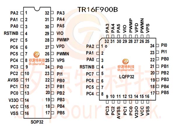
TR16F900B package:
SOP28/SOP32/SOP16/LQFP32/SSOP24/SSOP28/QFN28


Please submit your basic information, send an email to Sales@ChipSourceTek.com, or call us at 13823761625 (same number as WeChat), and we will contact you as soon as possible!

WeChat Official Account

WeChat Service
 Email
Email QQ
QQ 13823761625
