
Products
Products


TMI8118,TMI8118S
TMI8118/TMI8118S是一款为低输入电压下工作 的系统而设计的直流电机驱动集成电路,单通道低导通电阻。具备电机正转/反转/停止/ 刹车四个功能。
TMI8118/TMI8118S内置温度保护功能,当芯片 温度急剧升高,内部电路关断内置的功率开 关管,切断负载电流。
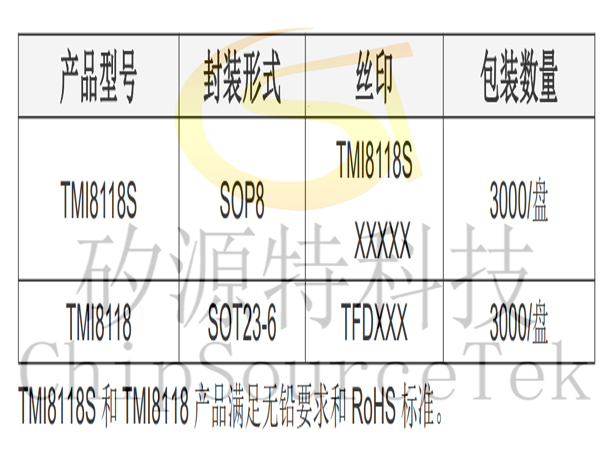
TMI8118S的封装形式是SOP8,TMI8118的封装形式是SOT23-6,符合ROHS规范, 引脚框架100%无铅。
TMI8118/TMI8118S内置温度保护功能,当芯片 温度急剧升高,内部电路关断内置的功率开 关管,切断负载电流。
TMI8118S的封装形式是SOP8,TMI8118的封装形式是SOT23-6,符合ROHS规范, 引脚框架100%无铅。
TMI8118/TMI8118S Description:
The TMI8118/TMI8118S is a DC motor driven integrated circuit designed for systems operating at low input voltage, with single channel low on-resistance. With motor forward/reverse/stop/brake four functions;
TMI8118/TMI8118S built-in temperature protection function, when the chip temperature rises sharply, the internal circuit turns off the built-in power switch tube, cut off the load current.
TMI8118S package form is SOP8, TMI8118 package form is SOT23-6, ROHS compliant, pin frame 100% lead-free.
TMI8118/TMI8118S Features:
Operating voltage range: 1.6V-7.2V
Very low standby current, 0.1μA typ.
Low RDS(ON) resistance:
0.53Ω SOP8 package, TMI8118S
0.55Ω SOT23-6 package, TMI8118
Integrated overheat protection
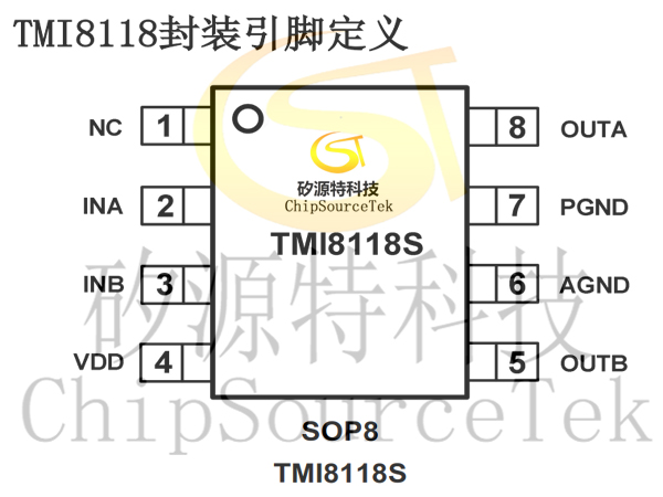
Package: SOP8 (TMI8118S)
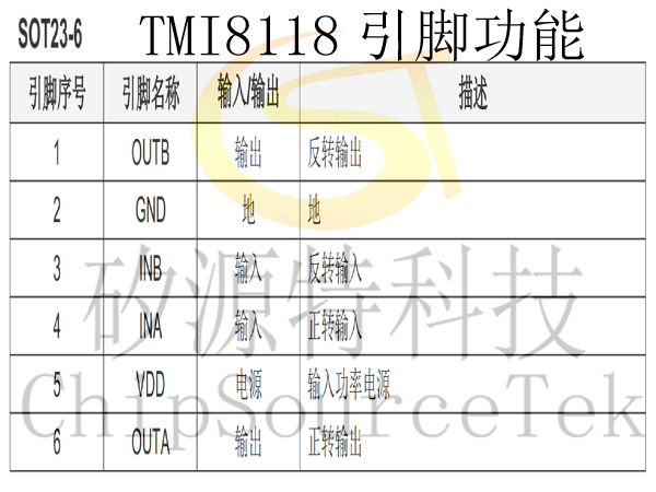
SOT23-6 (TMI8118)
Very low standby current, 0.1μA typ.
Low RDS(ON) resistance:
0.53Ω SOP8 package, TMI8118S
0.55Ω SOT23-6 package, TMI8118
Integrated overheat protection
Package: SOP8 (TMI8118S)
SOT23-6 (TMI8118)
TMI8118/TMI8118S Application:
Electric toy
Smart lock, padlock
Car clip
Dc brush motor drive:
Smart lock, padlock
Car clip
Dc brush motor drive:
TMI8118S Typical application circuit:

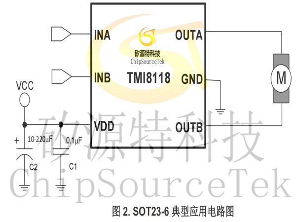
TMI8118 Typical application circuit:
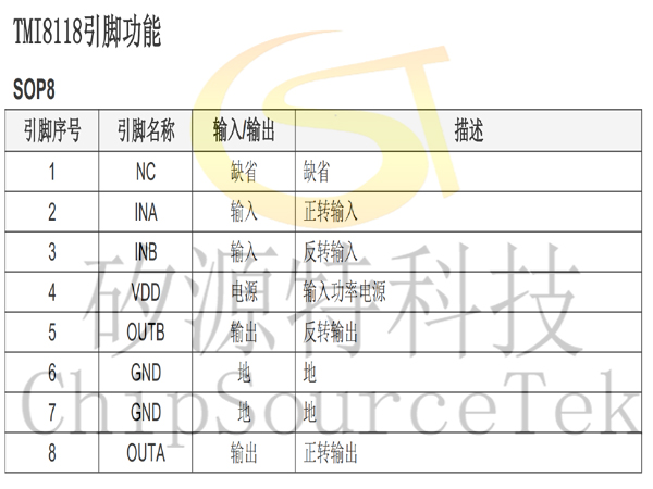
TMI8118S Package pin definition:

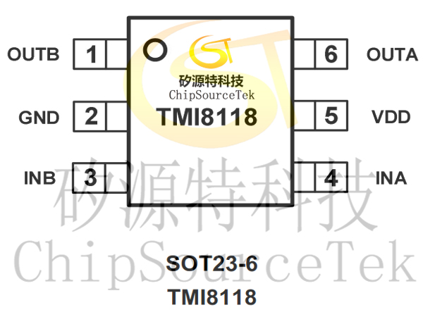
TMI8118 Package pin definition:
TMI8118/TMI8118S Ordering Information:
TMI8118S Pin features:
TM8118 Pin features:

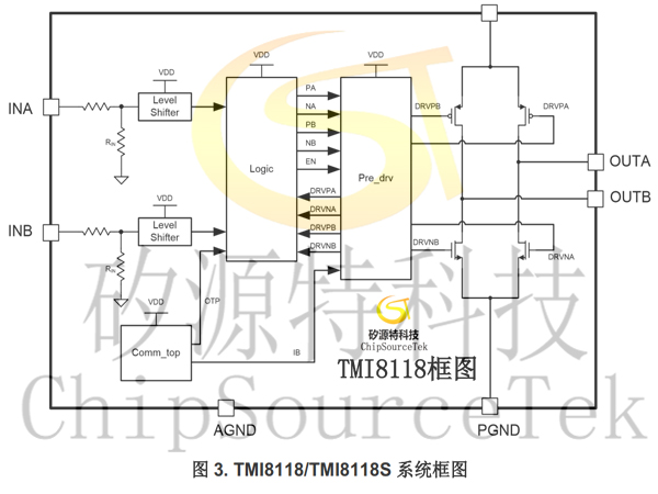
TMI8118/TMI8118S block diagram:

TMI8118/TMI8118S Application circuit precautions:
1. Do not ground the output pin OUTA/OUTB directly or power supply, because the over-temperature protection mechanism inside the IC is only for high temperature protection, if the peak current is too large, it will burn the IC;
2. Motor blocking transfer because of different motors have different peak currents, if the motor blocking peak current is too large may burn the IC;
3. VDD 电容必需尽可能的靠近芯片 VDD 和 GND 引脚。C1,C2 为 VDD 输入电容,主要作用如下:
3. The VDD capacitor must be as close to the chip VDD and GND pins as possible. C1 and C2 are input capacitors for VDD, and their main functions are as follows:
3.1. absorb the energy released by the motor to the power supply, stabilize the VDD power supply voltage, avoid the IC due to high impulse voltage and direct breakdown, with the function of filtering ripple and interference noise.
3.2. When the motor starts, the current can be released to help the motor start quickly.
3.3. The selection of VDD input capacitor C2 should be based on the voltage stability of VDD and the load current of the motor. If the voltage wave of VDD is larger or the load current of the motor is larger, the larger capacitance value must be selected.
3.4. On the PCB configuration, C1 and C2 capacitors should be as close to VDD as possible. When there is no input signal at the input INA or INB, do not leave the INA or INB pins empty. This prevents a weak leakage current at the P/N junction of the IC body from flowing through the pull-down resistor, which will cause the input potential of the suspended pin to change from low potential to high potential, resulting in incorrect circuit output signals.
TMI8118S Package size:
SOP8

TMI8118S Package size:
SOT23-6


Please submit your basic information, send an email to Sales@ChipSourceTek.com, or call us at 13823761625 (same number as WeChat), and we will contact you as soon as possible!

WeChat Official Account

WeChat Service
 Email
Email QQ
QQ 13823761625
