
In the design process of smart speakers, the design of power amplifiers and the recovery of AEC circuits are extremely crucial links, as they directly affect the sound quality, stability and overall performance of the speakers. Today, I'd like to share with you six design experiences and insights in these two aspects. Let you master the hardware design of smart speakers in one article: Key points of power amplifier and AEC sampling design.
I、Power Amplifier Type Showdown: Efficiency is the Key!
When faced with various types of power amplifiers, how to choose?
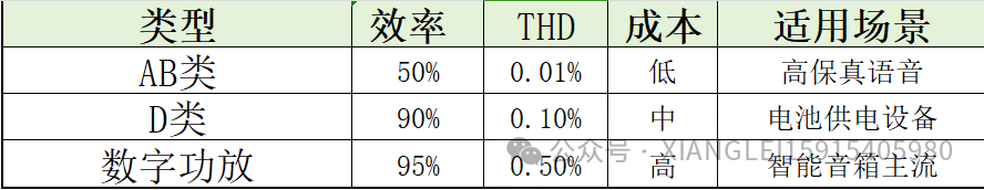
Class A (Pure Class A) :
It has the best linearity, pure and natural tone, and high fidelity. But is extremely inefficient (20%-30%) and generates a lot of heat。
Youdaoplaceholder0 class B:
The efficiency is relatively high (about 70%). However, there is "crossover distortion", and the sound quality is compromised.
Youdaoplaceholder0 class AB (Class a and b):
A compromise between Class A and Class B. The efficiency of needs improvement , but it has significantly improved the crossover distortion. It was a commonly used solution in fields such as automotive audio systems many years ago .
Youdaoplaceholder0 class D (two types of communication: analog input and digital signal) :
Based on the working principle of high-speed switching. Significant advantages: Extremely high efficiency! (Over 90%). It generates extremely little heat and can be made very compact in size.
Conclusion:
To achieve the high-efficiency goal of ≥85%, with cost constraints, the high-efficiency class D power amplifier is the best choice!
Pursuing more audio effect algorithms and efficiency - Digital power amplifiers are the best choice! Enable small-sized devices to also have powerful sound quality!
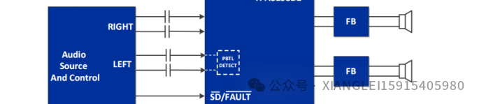
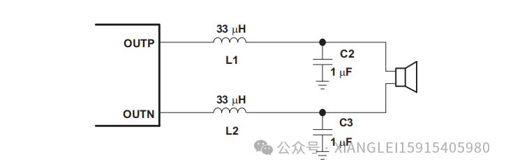
II、Key points of the circuit: power amplifier output filtering
Youdaoplaceholder0 output filter (core) :Since the output of Class D power amplifiers is a high-frequency PWM square wave, an LC low-pass filter is needed to restore it to a smooth audio signal. According to the Nyquist theorem, the cut-off frequency of the filter must be much higher than the highest frequency of the audio (usually >30kHz) in order to effectively filter out the PWM carrier (usually at several hundred kHz) without affecting the audio itself. The reason is that the upper limit of audio that the human ear can hear is 20kHz.
III、Key points of the circuit: The function of the AEC circuit for speaker signal recovery!
The full name of AEC is Acoustic Echo Cancellation. Its core function is to extract audio signals from the output end of the speaker for subsequent signal processing (such as echo cancellation, sound quality monitoring, feedback control, etc.).
Echo cancellation
In smart speakers, the microphone simultaneously picks up ambient sounds and the sounds played by the speakers. After extracting the speaker signals, algorithms can be used to cancel out this part of the "echo", making voice recognition more accurate.
Sound quality monitoring
Real-time collection of speaker signals, analysis of parameters such as distortion and noise, and feedback to the power amplifier for output adjustment;
Feedback control
In the power amplifier circuit, the harvested signal is used for closed-loop control to stabilize the output power or reduce distortion.
Ⅳ、Key design requirements - The mining circuit needs to address three core issues
Signal level adaptation
The voltage across the speaker is usually high (the output of the power amplifier may reach ±10V or even higher), and the audio input range of the subsequent processing chips (such as ADC, DSP) is limited (usually 0 to 3.3V), so the high voltage needs to be attenuated to a safe range.
Interference-free original circuit
The sampling circuit should not affect the normal operation of the speaker (such as the volume reduction caused by shunting), so the input impedance needs to be high enough to avoid "loading" into the speaker circuit.
Signal fidelity and noise reduction
Retain the audio signal (20Hz to 20kHz), and filter out high-frequency noise, power interference, etc.
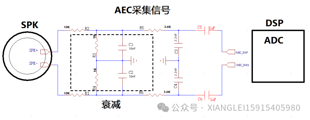
A typical circuit structure is usually composed of an attenuation network, a filter circuit, and a coupling unit. The following is the specific principle:
Attenuation network: Reduce the signal voltage. The audio signal at both ends of the speaker is an alternating voltage. By connecting resistors in series, a signal of ±10V can be attenuated to ±0.9V (within the ADC input range). The voltage divider resistor should be a high-precision 1% error and low-temperature drift resistor to avoid signal distortion. The total impedance must be high enough to ensure that the shunt to the speaker circuit can be ignored (without affecting the speaker current).
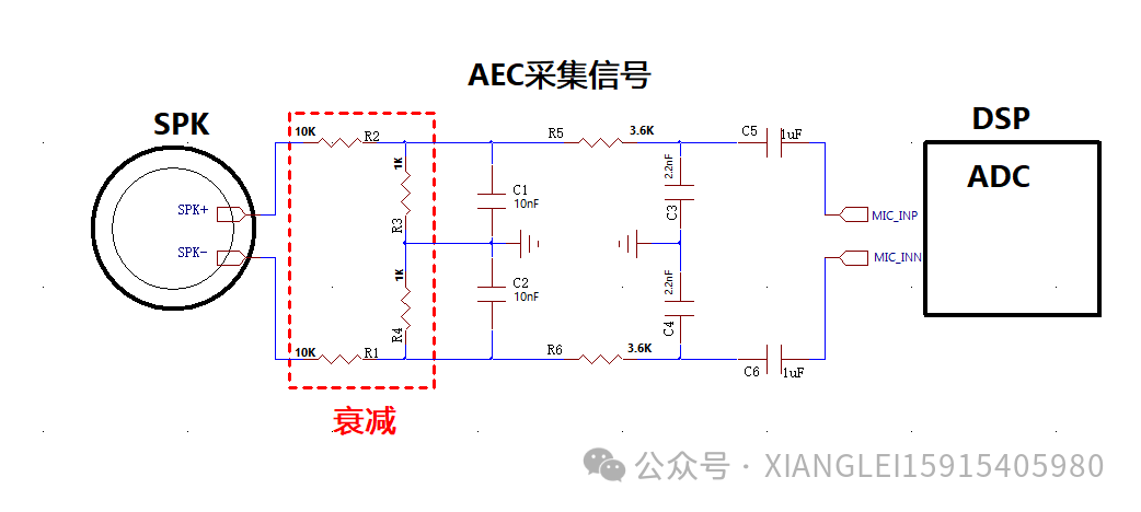
2. RC low-pass filter circuit: Retains the effective signal and filters out noise. The speaker is an inductive load (the voice coil has inductance), and the output of the power amplifier may be mixed with high-frequency noise (such as interference from switching power supplies and radio frequency interference). It is necessary to extract pure audio signals (20Hz to 20kHz) through a filter circuit. Calculation formula: fc=1/(2πrc). The cut-off frequency can filter out high-frequency noise above 20kHz and retain the audio signal.
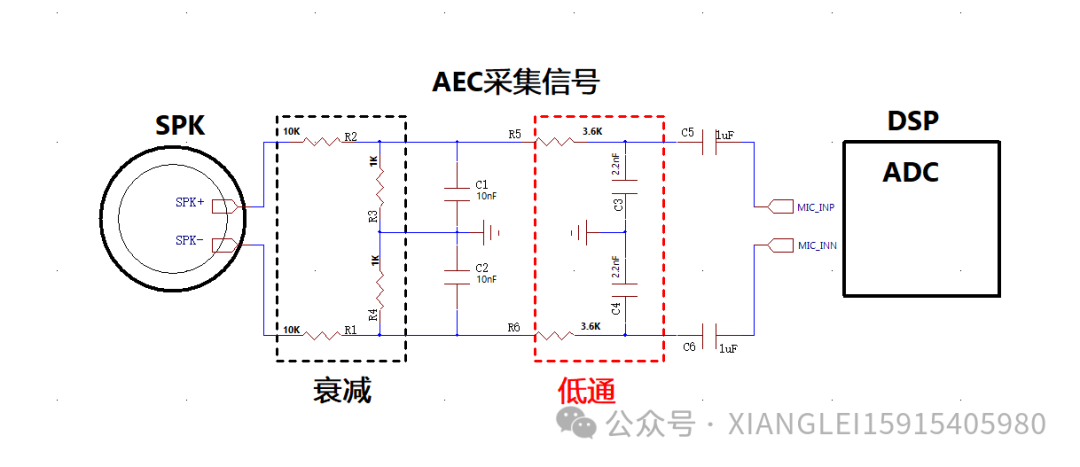
3. Coupling: Adapt the signal polarity of the subsequent circuit. The speaker signal is an AC signal, and there are other interference signals that need to be coupled to the ADC chip through capacitors.
Ⅳ、The workflow of complete speaker signal acquisition is:
plaintext speaker output terminal (high-voltage AC signal)
→ Attenuation network: Resistors divide the voltage to reduce it to a safe range.
→ Filter circuit: RC low-pass/high-pass, filter out noise, and retain 20Hz to 20kHz audio.
→ Input into ADC/DSP (convert analog signals to digital signals)
→ Algorithm processing (such as echo cancellation, distortion analysis, etc.)
Ⅳ、Key parameters and design considerations
Attenuation ratio calculation
Calculate the maximum voltage of the root speaker and the upper limit of the ADC input. For example, the maximum voltage of the root speaker is ±30V, and the upper limit of the ADC is 3.3V. The attenuation ratio should be ≥30:3.3≈9:1 (in practice, 10:1 is taken to leave redundancy).
Impedance matching:
The input impedance of the feedback circuit should be ≥ 10 times the impedance of the speaker (for example, for a 4Ω speaker, the feedback input impedance should be ≥40Ω, and in practice, 10kΩ or above is usually used), to avoid the impact of shunting on the speaker volume.
Grounding treatment
The recycling circuit needs to be grounded at a single point to avoid sharing the ground with the power amplifier and microphone circuits and introducing noise.
Dynamic range
The peak-to-peak value of the attenuated signal should be less than the full scale of the ADC (for example, for a 3.3V ADC, the peak-to-peak value of the signal should be ≤3V) to avoid clipping distortion. Usually, the audio signal is less than 1V.
Through the above design, the speaker signal recovery circuit can accurately extract audio signals without interfering with the operation of the speaker, providing original data support for subsequent functions such as echo cancellation and sound quality optimization.
Key summary: AEC circuits vary for different DSP chips!
For chips with ADC input, the speaker directly uses an attenuation circuit and is then connected to the analog audio input port of the chip.
(PS: Some chips internally support ADC output detection, and the software comes with an AEC function, which is more convenient.)
For chips without ADC input, such as I2S communication, an ADC conversion chip needs to be added.
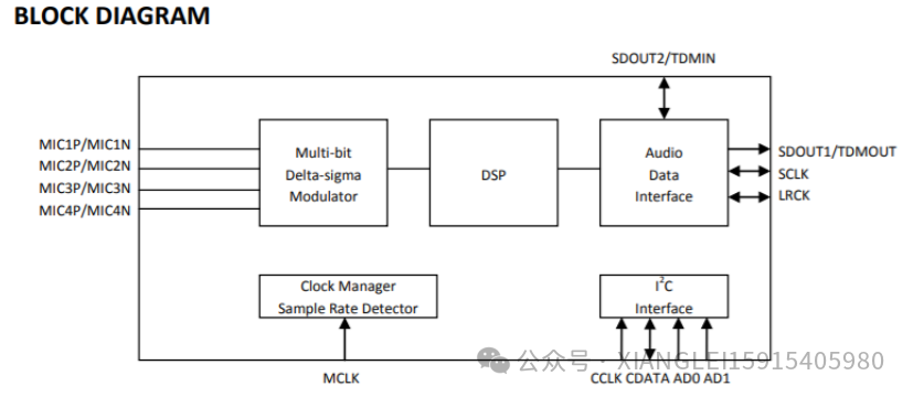
The AEC recovery signal is input to the ADC chip through differential traces.
MIC signals are usually at the mV level. Please note that the input signal should not exceed the maximum range of the chip input to avoid signal clipping distortion!
免责声明: 本文章转自其它平台,并不代表本站观点及立场。若有侵权或异议,请联系我们删除。谢谢! Disclaimer: This article is reproduced from other platforms and does not represent the views or positions of this website. If there is any infringement or objection, please contact us to delete it. thank you! |

WeChat Official Account

WeChat Service
 Email
Email QQ
QQ 13823761625
