
ESD damage may be caused by excessive voltage, excessive current, or both. High voltage may cause the gate oxide to break down, while excessive I 2R May lead to junction failure and melting of the metallization trace. As the manufacturing size continues to shrink (Intel's Haswell uses a 22nm process), the voltage and current levels that may cause ESD-related failures also decrease accordingly. This makes it difficult to provide even relatively low levels of on-chip ESD protection; Therefore, the focus has shifted to individual ESD protection devices.
Changing the application environment will bring problems
The popularity of laptops, mobile phones, MP3 players, digital cameras and other handheld mobile devices has brought special problems to high-speed differential interfaces such as USB 3.1, HDMI 2.0, DisplayPort, etc. In these uncontrolled environments, owners often touch the pins of I/O connectors when connecting and disconnecting cables. When users plug cameras, games and other devices into their USB and video ports, the devices are constantly subjected to ESD pressure.
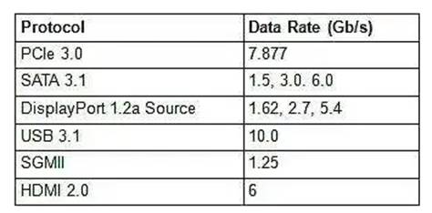
Protocol Data Rate (Gb/s) PCIe 3.0 7.877 SATA 3.1 1.5, 3.0.6.0 DisplayPort 1.2a Source 1.62, 2.7 5.4 USB 3.1 10.0 SGMII 1.25 HDMI 2.0 6 Table 1: Some Common high-speed Serial interfaces
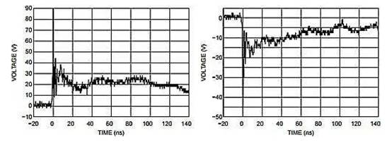
IEC 61000-4-2 is the industry standard for system-level ESD testing, aiming to replicate the discharge situation of the system by live personnel in the end-user environment. The purpose of system-level testing is to ensure that the finished product can survive during normal operation, and it is usually assumed that users will not take any ESD preventive measures when using the product. The resulting electrostatic discharge can reach 16A within 30 ns (IEC 61000-4-2 Class 4, 8kV contact discharge).
ESD protection technology.
In a high-speed serial interface, it is not enough for an ESD protection device to merely clamp ESD pulses: it must do so without compromising the signal integrity of the high-speed link.
As the speed increases, it is crucial for the interface to maintain impedance matching throughout the signal path. Any impedance mismatch will cause line reflection, thereby increasing jitter and possibly damaging signal quality. Therefore, high-speed serial interfaces require strict capacitance limits for any external components in the signal path.
Adding the required ESD protection will also increase unnecessary additional capacitance. For the traditional ESD equipment architecture, as the protection level increases, the equipment capacitance also increases, forcing designers to make a choice between signal integrity and ESD protection. Semiconductor diodes have many ideal characteristics, such as low clamping voltage, fast turn-on time and better reliability, but until recently, their capacitance has been higher than that of other architectures.
Recently, manufacturers have launched diode protection devices with extremely low capacitance specifically designed for high-speed applications. For example, NXP's PUSB3FR4 is designed to protect high-speed interfaces, such as the 10 Gbps SuperSpeed USB 3.1. This device consists of four ESD protection diode structures and is packaged in a lead-free small DFN2510A-10 (SOT1176-1) plastic package.
All signal lines are protected by special diode configuration and can provide a line capacitance of 0.29 pF. The diode adopts a fast recovery structure to provide protection for downstream components and prevent contact ESD voltages up to +/-15 kV, exceeding IEC 61000-4-2 level 4.
Similar PUSB3FR6 has six ESD devices, providing system-level protection for the interface combination of USB 2.0 and USB 3.1, which is a feature of the new USB Type C connector.
ON Semiconductor is also active in this market: Its ESD7008 adopts the UDFN18 package and provides ESD protection for 4 differential pairs (8 lines), with a typical ground capacitance value of 0.12pF.
Many parasitic components on the PCB may reduce the overall ESD performance of the system. Therefore, it is necessary to optimize the placement of ESD protection devices and the PCB layout to achieve the best ESD performance.
The following are some suggestions:
Parasitic inductance must be minimized as much as possible by shortening the ground path that returns to the GND vias.
Symmetrical layout can also reduce parasitic inductance. It is important to connect the connector to one side of the ESD device and the transceiver to the other side.
To prevent ESD from spreading on the PCB, ESD protection devices must be placed as close as possible to the ESD source.
Since ESD stress can propagate on both sides of the interface cable, protective devices need to be equipped at each end of the cable.
For high-speed ESD protection equipment, flow-through packaging is used to facilitate correct layout practices. Figure 2 shows the pin arrangement of ST's HSP061-4NY8, which provides 4-wire ESD protection for HDMI, USB 3 and similar interfaces. The ground of the I/O capacitor is 0.6pF, and the differential impedance is 100 Ω (typical value) under the HDMI specification.
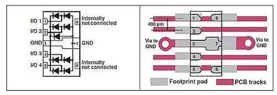
HSP061-4NY8 Pin Distribution and flow-through Package (Source: ST)
免责声明: 本文章转自其它平台,并不代表本站观点及立场。若有侵权或异议,请联系我们删除。谢谢! Disclaimer: This article is reproduced from other platforms and does not represent the views or positions of this website. If there is any infringement or objection, please contact us to delete it. thank you! |

WeChat Official Account

WeChat Service
 Email
Email QQ
QQ 13823761625
