
Ⅰ、Brief Introduction
The I2C (Inter-Integrated Circuit) bus is a two-wire serial bus developed by Philips,Used for connecting microcontrollers and their peripheral devices. The I2C bus originated in the 1980s and was initially developed for audio and video devices.
Due to its simplicity, it is now widely used in the connection between microcontrollers and various functional modules. It can be said that for those who are learning single-chip microcomputers, it is a must-encounter after getting started.
The I2C bus has actually become an international standard implemented on over 100 different ics and has been licensed by more than 50 companies. Due to its simplicity and wide application, its functions are increasingly failing to meet people's requirements, and its speed has also increased from the original 100 kbit /S to a fast mode. Its speed reaches 400Kbit/S. Later, a high-speed mode was added, and its speed even reaches 3.4Mbit/S.
Ⅱ、Functions and Features
The I2C bus is a bidirectional two-wire bus used for the connection between IC devices,The so-called bus can hold as many devices as possible and be connected by just two wires, taking up very little space. The length of the bus can be as high as 25 feet and it can support 40 components at a maximum transmission rate of 10Kbps.
Another advantage of it is that it has multiple main controllers. Any device capable of receiving and sending can serve as the main controller. Of course, multiple main controllers cannot work simultaneously.
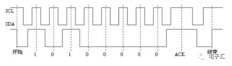
The I2C bus has two signal lines, one being the SDA (data line) and the other the SCL (clock line).At any time, the clock signal is generated by the main control device.
During the process of data transmission on the I2C bus,There are mainly three types of control signals: the start signal, the junction signal, and the response signal.
Initial signal: When SCL is at a high level and SDA changes from a high level to a low level, data transmission begins.
End signal: When SCL is at a high level and SDA changes from a low level to a high level, the data transmission ends.
Response signal: After receiving 8-bit data, the device receiving the data sends a low-level signal to the device sending the data, indicating that the data has been received. This signal can be emitted by the main control device or the driven device. In conclusion, it is sent by the device that receives the data.
Among these signals, the starting signal is necessary, while the ending signal and the response signal can both be omitted.
Ⅲ、Basic operations
Below, we will introduce the basic operation of I2C using ATMEL's AT24C02.
AT24C02 is a low-power CMOS serial EEPROM from ATMEL Corporation of the United States. It contains 256× 8-bit storage space and features a wide operating voltage range (2.5 to 5.5V), a large number of erase and write cycles (more than 10,000 times), and a fast write speed (less than 10ms). He is always the driven device in the system.
The main operations on AT24C02 are: byte read, byte write, page read, and page write
First, send the start signal, as shown in the following figure. After the start signal, there must be control words.
The control word format is as follows. The first four bits are the device type identifier (different chip types have different definitions; for EEPROM, it is generally 1010), followed by three bits for the chip selection, that is, three address bits, and the last bit is the read/write control bit. When it is 1(Input), it is a read operation, and when it is 0(Output), it is a write operation.
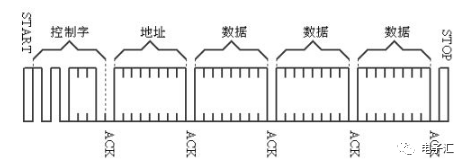
After the control word comes the corresponding operation, reading or writing. Do not end it because the operation is not yet completed. If it ends, it is equivalent to giving up the operation.
Let's first look at the write operation. Write operations are divided into two types: byte write and page write. For page write, it varies depending on the number of bytes loaded at one time on the chip. AT24C02 has 8 bytes. After each byte is written, the address is automatically increments by 1.
The sequence of address, response and data transmission for page write is shown in Figure 3. Byte write can be regarded as a page write with only one byte, that is, it stops after writing one piece of data.
Note: Writing once takes a certain amount of time, usually 10ms. Please wait for this operation to complete. The sequence is as shown in the following figure.
Note: For AT24C02, an address must also be written after the control word. This address serves as the starting address for future reading and writing.
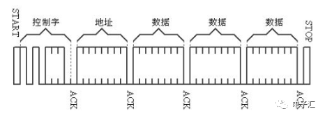
There are three basic read operations: current address read, random read and sequential read。The three operation methods are similar, but the number of data read is different. It can continuously read up to 8 bytes. Figure 4 shows the sequence diagram of sequential reading. A total of four data are read in the figure. It should be noted that the current address is not the desired one. If it is not the desired one, a write operation can be used to rewrite the address.
It is extremely important that after reading each piece of data, the SDA must be set low as a response. Otherwise, only one piece of data can be read. For the subsequent data, due to receiving a non-response signal, AT24C02 will consider it an error and stop the operation.
It should be particularly noted that when SCL is at a low level, the data is variable. Therefore, readings can only be taken when SCL is at a high level.
Ⅳ、Example program(51 assembly, the test single-chip microcomputer is AT89C51, with a 12M crystal oscillator)
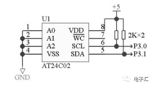
The circuit connection is shown in Figure 5, where A0, A1, and A2 are address lines. In this example, all of them are grounded, so they are all 0. Since SCL and SDA are open-drain outputs, a pull-up resistor needs to be added when in use.
五、Conclusion
The matters needing attention in the application of I2C bus can be summarized as follows:
●Operate strictly in accordance with the requirements of the sequence diagram;
●If it is connected to the interface of a single-chip microcomputer with an internal pull-up resistor on the port line, an additional pull-up resistor does not need to be added.
●In the program, to match the corresponding transmission rate, a certain delay can be added after the instruction for port line operation using the NOP instruction.
●To reduce unexpected interference signals and rewrite the data within the EEPROM, an external write protection pin (if any) can be used, or a flag word can be written in the unused space within the EEPROM. Perform a check each time the EEPROM is powered on or reset to determine if it has been accidentally rewritten.
免责声明: 本文章转自其它平台,并不代表本站观点及立场。若有侵权或异议,请联系我们删除。谢谢! Disclaimer: This article is reproduced from other platforms and does not represent the views or positions of this website. If there is any infringement or objection, please contact us to delete it. thank you! |

WeChat Official Account

WeChat Service
 Email
Email QQ
QQ 13823761625
