
Background information
Linear regulators are widely used in many modern electronic systems. Although low dropout (LDO) linear regulators rarely become the most expensive system components, from a cost/benefit perspective, these regulators are often one of the most valuable components. One of the tasks of LDO is to protect downstream loads from damage caused by harsh environmental conditions, such as temperature offset, voltage transients, power supply noise, voltage reverse, current surges, and EMI or ESD. In short, its design must be robust and reliable, and incorporate all the protective functions necessary to mitigate environmental impact while safeguarding the load. Many low-cost LDO linear regulators do not contain necessary protection functions, thus failing to provide protection. They often not only cause damage to the regulator but also result in load damage.
For those who need to protect expensive and sensitive loads, an image sensor system is a typical example. Image sensors typically contain cutting-edge and expensive digital ics that acquire images and directly convert them into digital images. The two most popular image sensors are charge-coupled devices (CCD) and CMOS imagers. Various devices such as endoscopes and security cameras all contain image sensors.
Some applications require controlling the power supply cycle when powered on and off. In multi-rail systems, FPgas, ASics, DSPS, microprocessors and other digital ics require that multiple voltage rails must be started and turned off in a specific sequence. Otherwise, these ics may be damaged, or the power-on reset logic of the system may have errors. If not sorted correctly, disastrous consequences may occur. For systems that must control the output state, such as military, avionics or aerospace high-reliability systems, they are very typical examples, especially when the power supply voltage needs to be continuously cycled on and off.
The LDO can utilize the active output discharge function to meet the system's power-off requirements. The active output discharge function enables the LDO's output to discharge rapidly without relying on the LDO's load or the LDO's resistor voltage divider to discharge the output. If the input voltage is removed or if the turn-off function is activated, the LDO with active output discharge function can quickly lower the output voltage by an NMOS switch. The main advantage of devices with active output discharge function is that when power is cut off, the output remains in a known state. Regardless of the load state, the output of this type of device always discharges rapidly as expected. For applications that require accurate power sequencing when turned off (such as image sensors and microcontrollers), it is very important to be able to actively output discharge.
Comparison of low-dropout linear regulators (Ldos) with other regulators
Low-voltage reduced-voltage type conversion and voltage stabilization can be achieved through various methods. Switching regulators operate efficiently over a wide voltage range, but they require magnetic components and capacitors to function, thus occupying relatively large space on the circuit board. Charging pumps (or switching capacitor voltage converters) can be used to achieve lower voltage conversion, but their output current capacity is limited, and they require external capacitors to operate and stabilize. Low-dropout linear regulators are usually less efficient, but they generate less noise and are easier to be used in reduced-voltage applications. However, modern design methods and chip manufacturing processes have enabled low-dropout linear regulators (Ldos) to further penetrate into the field of step-down applications. Nowadays, low-dropout linear regulators feature ultra-fast transient response, low dropout voltage, low-voltage operation (output typically as low as 0.6V), large output current capability, and the ability to operate with a single power supply.
At present, the first-generation fast, high-current, low-voltage digital ics (such as FPGA, DSP, CPU and ASIC) have very strict requirements for the power supply that powers the core and I/O channels. However, from the perspective of power supply, these digital ics are not stable enough. Traditionally, high-efficiency switching regulators have been used to power such devices, but switching regulators may have potential noise interference issues as well as transient response and layout limitations. Therefore, LDO, as an alternative device, is finding its place in such applications and other low-voltage conversion systems. Due to recent product innovations and functional enhancements, the trend is changing, and the new LDO requires almost no compromise in performance.
LDO Design Challenge
A large number of industrial standard linear regulators operate with a single voltage source at a low dropout, but most regulators cannot simultaneously provide very low voltage and output noise conversion (output as low as 0.6V), a wide input/output voltage range, and extensive protection functions. PMOS LDO can operate with a single power supply at a low dropout, but due to the limitations of the characteristics of the path transistor VGS, the input voltage cannot be very low. Devices based on NMOS provide fast transient responses, but two power supplies are required to bias the device. NPN regulators offer a wide range of input and output voltages, but they require two power supply voltages or a large voltage difference. In contrast, if the architecture of a PNP regulator is properly designed, it can achieve a very low voltage drop, a very high input voltage, low noise and low-voltage conversion with a single power supply, and can also provide reliable protection.
With the continuous reduction of process technology nodes, modern digital ics need to operate at lower voltages. For many existing input voltage rails, operating at a larger current and a lower output voltage means that the power consumption of the linear regulator will increase. The increased power consumption is directly converted into heat. Therefore, the latest packaging method needs to be adopted to minimize the temperature rise inside the voltage regulator and limit the heat issue of the application. In addition, a linear regulator capable of operating at a low dropout (minimizing the difference between input and output voltages while maintaining regulation and stability of the output) can reduce power consumption, thereby alleviating the heat issue.
Two more challenges are the need for a high power supply ripple rejection ratio (PSRR) and low output voltage noise. Devices with a high power supply ripple suppression ratio can easily filter out and suppress noise from the input, generating clean and stable output. Furthermore, devices that output very low voltage noise over a wide bandwidth are beneficial for today's voltage rails, as noise sensitivity is a factor that needs to be considered for modern voltage rails. High current and low output voltage noise are obviously necessary performance requirements.
Some industrial Ldos offer active output discharge functions to protect the load. However, the existing solutions only start when the device is turned off. So far, it is still very difficult to find a circuit design with a "dual" function to actively output and discharge, that is, this function can also be activated when the input voltage is pulled low.
A new single-power linear regulator
Obviously, an active output discharge LDO should have the following characteristics:
• Operate with a single power supply (for ease of use)
• Fast transient response time
•It operates within a wide range of input/output voltages
•It can provide a very large output current
•Low output noise
•Operate at a very low pressure difference
• Excellent thermal performance
•It has a high PSRR over a very wide frequency range
•The active output discharge circuit has a complete dual function - it is effective when either SHDN or VIN is pulled low
Fortunately, Linelite has recently launched the 500mA LT3066 low-dropout linear regulator with active output discharge function. This device possesses all the necessary attributes mentioned above. Some applications require that the output state is known when the device is turned off, and the design of LT3066 meets this requirement. Its output always discharges rapidly as expected, regardless of the state of the load.
The LT3066 is a high-voltage, low-noise, low-dropout linear voltage regulator that offers precise and programmable current limiting, active discharge, a good power supply marking, and a better power supply rejection ratio (PSRR). This device provides an output current of up to 500mA and a differential voltage of 300mV when fully loaded. The LT3066 contains an internal high-voltage NMOS pull-down circuit to discharge the output voltage when the SHDN pin is pulled low or the input voltage is disconnected. For applications that require power regulation during startup and shutdown (such as high-end imaging sensors or microcontrollers), this fast active output discharge function helps protect the load.
The LT3066 has a very wide input voltage range of 1.8V to 45V, and the output voltage is adjustable within the range of 0.6V to 19V. A single REF/BYP pin capacitor provides a soft-start function, enabling the device to operate at a low noise of only 25µVRMS within a bandwidth of 10Hz to 100kHz. The output voltage tolerance varies with voltage, load and temperature to a highly accurate ±2%. Another INFILT pin capacitor improved the PSRR by 15dB to 30dB in the frequency range of 20kHz to 1MHz, and reached 60dB at 1MHz.
The LT3066 operates with a small, low-cost ceramic output capacitor of as low as 3.3µF. The PWRGD marking of this device indicates that the output is in a stable state. The LT3066 precisely sets the external current limit with a resistor (±10% over the entire temperature range). In addition, the internal protection circuits of the LT3066 include battery reverse protection, current reverse protection, return current limit and overheat limit. The active discharge circuit provides a safe operating area (SOA) return function to protect the pull-down NMOS, keeping the OUT voltage above 6V and offering a wide range of absolute maximum ratings for OUT pins: -1V to +20V. As shown in Figure 1, this device features A wide input and output voltage range, A fast transient response, and a low quiescent current of 64µA (during operation) and <3µA (during shutdown). Therefore, it becomes an excellent choice for industrial power supplies, avionics system power supplies, automotive power supplies, battery-powered systems and instruments that require optimal operating time, as well as highly reliable power supplies that need extensive protection.
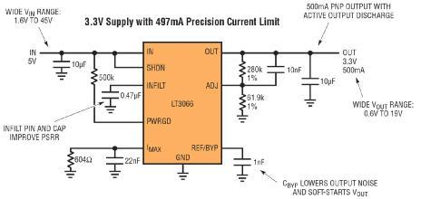
WIDE VIN RANGE: 1.6V TO 45V: A very wide VIN range: 1.6V to 45V
IN: Input
INFILT PIN AND CAP IMPROVE PSRR: INFILT pins and capacitors improve PSRR
500mA PNP OUTPUT WITH ACTIVE OUTPUT DISCHARGE: 500mA PNP output, capable of actively discharging
OUT: Output
WIDE VOUT RANGE: 0.6V TO 19V: A very wide VOUT range: 0.6V to 19V
CBYP LOWERS OUTPUT NOISE AND SOFT-STARTS VOUT: CBYP reduces the output noise and makes VOUT soft-start
Figure 2 shows that the 500mA LT3066 with active output discharge function is superior to the similar LT3065 (500mA, without active output discharge function)
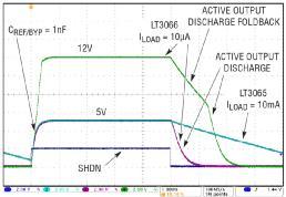
ACTIVE OUTPUT DISCHARGE: Active output discharge
The LT3065 has A 10mA load, while the LT3066 is only loaded by a resistor voltage divider with a set output voltage (in this case, 10μA). Even if a very light load is applied to the output of the LT3066, the output voltage will discharge rapidly due to the active output discharge function provided by this device. In contrast, the output capacitor of the LT3065 discharges only from the 10mA load connected to it, and the discharge speed is much slower.
For output voltages above approximately 7V, the LT3066 implements active output discharge return. As a result, the drive of the transistor used for active output discharge is reduced, which can limit the power consumed by the device. Due to the occurrence of return-back, it can be seen on the oscilloscope display that the 12V waveform of the LT3066 does not discharge so fast from 12V to 7V. When the output voltage is very high and large capacitors are used, or in case of a fault that short-circuits the output to a very high voltage, such a discharge rate can protect the LT3066 from damage.
T he main advantage of devices with active output discharge function is that when the device is turned off, the output is in a set known state. The output always discharges rapidly as expected, regardless of the state of the load. This feature is very important for applications that require precise power sequencing during downtime.
Improvement of PSRR performance
Compared with other devices in the LT306x series, the LT3066 enhances PSRR performance through the INFILT pin. The INFILT pin is a separate input pin that powers the error amplifier and the reference. This pin is connected to the IN pin through an internal 140Ω resistor. By connecting a decoupling capacitor between the INFILT pin and ground, an RC filter is formed to reduce the input power ripple of the error amplifier and the reference. Connecting a 0.47μF decoupling capacitor to the INFILT pin can improve the PSRR by up to 30dB at frequencies above 10kHz. If input filtering is not required, then connect the INFILT pin to the IN pin. Figure 3 shows the improvement of PSRR performance of LT3066 compared with LT3065.
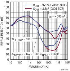
FREQUENCY: Frequency
The complete LT306x series
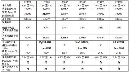
Not all applications require active output discharge to protect sensitive loads, nor do all applications demand an output current as high as 500mA. Therefore, Lynx has also developed another five devices in the LT306x series to offer an attractive product portfolio. The devices in this series have the following features: High input and output voltages, low dropout voltage, low output voltage noise performance, extensive protection functions, fast response, and a very wide output current range of 100mA to 500mA. Some of the devices have the function of active output discharge, while others do not have this function. The following Table 1 highlights the differences among various devices in the LT306x series.
Conclusion
The new circuit design method and the improved chip manufacturing process have enriched the performance characteristics of transistor Ldos based on the PNP path. The Ldos provided by suppliers such as Linlierte feature reliable protection functions, a wide range of input and output voltages, low output noise and fast response, and can operate with a single voltage source at low dropout. The new LT306x series features six devices with an output current range of 100mA to 500mA. Among them, three devices also offer a new complete dual-action active output discharge function, which is highly suitable for use in image sensors and high-reliability systems to protect sensitive and expensive loads while achieving precise power sequencing.
免责声明: 本文章转自其它平台,并不代表本站观点及立场。若有侵权或异议,请联系我们删除。谢谢! Disclaimer: This article is reproduced from other platforms and does not represent the views or positions of this website. If there is any infringement or objection, please contact us to delete it. thank you! |

WeChat Official Account

WeChat Service
 Email
Email QQ
QQ 13823761625
