
Developing a mobile handheld device with a touch-screen human-machine interface is a complex design challenge, especially for projective capacitive touch screen designs, which represent the current mainstream technology for multi-touch interfaces. The projected capacitive touch screen can pinpoint the position of the finger to touch the screen, and it determines the finger position by measuring small changes in capacitance. A key design issue to consider in such touchscreen applications is the impact of electromagnetic interference (EMI) on system performance. Performance degradation caused by interference may have adverse effects on touch screen design. This paper discusses and analyzes these interference sources.
Projected capacitive touch screen structure
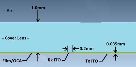
Typical projective capacitive sensors are mounted under a glass or plastic cover plate. Figure 1 shows a simplified side view of a double-layer sensor. The transmitting (Tx) and receiving (Rx) electrodes are connected to a transparent indium tin oxide (ITO) to form a cross matrix, with each TX-RX node having a characteristic capacitance. The Tx ITO is located below the Rx ITO and is separated by a polymer film or optical adhesive (OCA). As shown, the direction of the Tx electrode is from left to right, and the direction of the Rx electrode is from the outside of the paper to the inside of the paper.
Let us temporarily ignore the interference factors, to analyze the work of the touch screen: the operator's finger nominal ground potential. The Rx is held at ground potential through the touch screen controller circuit, while the Tx voltage is variable. The varying Tx voltage causes the current to pass through the TX-RX capacitor. A carefully balanced Rx integrated circuit isolates and measures the charge entering Rx, and the measured charge represents the "mutual capacitance" connecting Tx and Rx.
Sensor status: Not touched
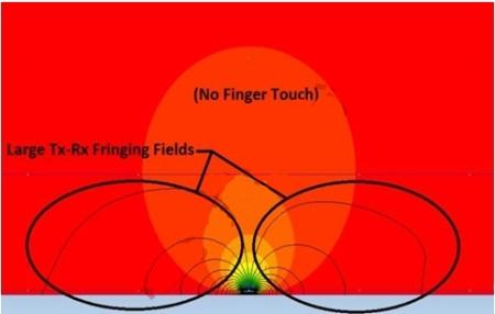
Figure 2 shows a diagram of the magnetic field lines in the untouched state. Without the touch of a finger, the Tx-Rx magnetic field line takes up a considerable amount of space inside the cover plate. The edge magnetic field lines project outside the electrode structure, hence the term "projective capacitance".
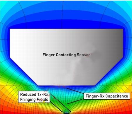
When the finger touches the cover plate, magnetic force lines form between the Tx and the finger, and these magnetic force lines replace a large number of TX-RX edge magnetic fields, as shown in Figure 3. In this way, finger touch reduces the Tx-Rx mutual capacitance. The charge measuring circuit recognizes the changing capacitance (△C) and thus detects the finger above the Tx-Rx node. By measuring △C at all the intersections of the Tx-Rx matrix, a touch layout of the entire panel can be obtained.
Figure 3 also shows another important effect: the capacitive coupling between the finger and the Rx electrode. Through this path, electrical interference may be coupled to Rx. Some degree of finger-RX coupling is inevitable.
The interference of the projective capacitive touch screen is generated through the imperceptible parasitic path coupling. The term "ground" can often be used to refer either to a reference node of a direct current circuit or to a low-impedance connection to the ground: the terms are not the same. In fact, for portable touch screen devices, this difference is the root cause of touch coupling interference. For clarification and to avoid confusion, we use the following terms to evaluate touch screen interference.
Earth: Connected to the earth, for example, through the ground wire of a 3-hole AC power outlet.
Distributed Earth: Capacitive connection of objects to the earth.
DC Ground: The DC reference node for portable devices.
DC Power: Battery voltage for portable devices. Or the output voltage of a charger connected to a portable device, such as a 5V Vbus in a USB interface charger.
DC VCC(DC VCC Power Supply) : A stable voltage that powers the electronics of portable devices, including LCD and touch screen controllers.
Neutral: AC power supply loop (nominal ground potential).
Hot(Live line) : AC power supply voltage, applying electrical energy to the neutral line.
LCD Vcom coupling to touch screen receiving line
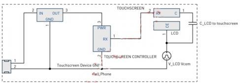
The portable touch screen can be mounted directly onto the LCD display. In a typical LCD architecture, the liquid crystal material is offset by transparent upper and lower electrodes. Multiple electrodes at the bottom determine the multiple single pixels of the display; The upper common electrode is a continuous plane covering the entire visible front end of the display, which is biased at the voltage Vcom. In a typical low-voltage portable device, such as a mobile phone, the AC Vcom voltage is a square wave oscillating back and forth between DC ground and 3.3V. The AC Vcom level is usually switched once per display line, so the resulting AC Vcom frequency is 1/2 the product of the display frame refresh rate and the number of lines. A typical portable device may have an AC Vcom frequency of 15kHz. Figure 4 shows the LCD Vcom voltage coupling to the touch screen.
To reduce architectural costs and achieve better transparency, the single-layer touchscreen installs the Tx and Rx arrays on a single ITO layer and connects each array in turn via a separate bridge. Therefore, the Tx array cannot form a shield between the LCD Vcom plane and the sensor Rx electrode. This can lead to serious Vcom interference coupling.
Charger interference
Another potential source of touchscreen interference is the switching power supply of a power-powered phone charger. Interference is coupled to the touch screen by fingers, as shown in Figure 5. Small phone chargers usually have AC power firewire and neutral wire inputs, but no ground connection. The charger is securely isolated, so there is no DC connection between the power input and the charger secondary coil. However, this still creates capacitive coupling by isolating the transformer with a switching power supply. The charger interference forms a return path by touching the screen with a finger.
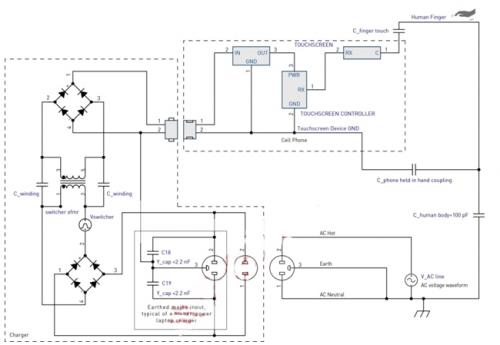
Charger coupling impedance
The charger switch interference is generated by coupling the leakage capacitance (about 20pF) in the primary to secondary windings of the transformer. This weak capacitance coupling can be compensated for by parasitic parallel capacitors that appear relatively distributed in the charger cable and the receiving device itself. When picking up the device, the shunt capacitance will increase, which is usually enough to eliminate the charger switch interference and avoid interference affecting touch operation. When the portable device is connected to the charger and placed on the desktop, and the operator's fingers are only in contact with the touch screen, a worst-case interference from the charger will occur.
Charger switch interference component
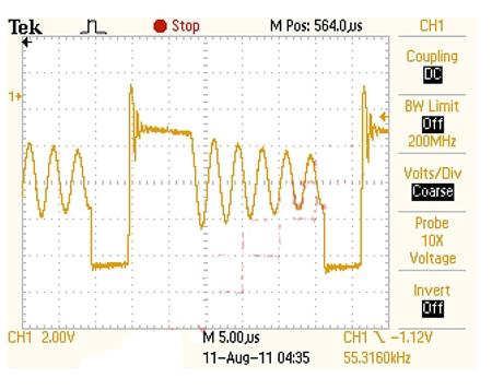
A typical mobile phone charger uses a flyback circuit topology. The interference waveform generated by such chargers is complex and varies greatly from charger to charger, depending on circuit details and output voltage control strategy. Interference amplitudes are also highly variable, depending on the design effort and unit cost invested by the manufacturer in switching transformer shielding. Typical parameters include:
Waveform: including complex pulse width modulated square wave and LC ringing waveform. Frequency: 40~150kHz under rated load, when the load is very light, the pulse frequency or jump cycle operation drops below 2kHz. Voltage: up to half of the peak power supply voltage =Vrms/√2.
Charger power interference component
At the front end of the charger, AC power supply voltage rectification generates a high voltage rail of the charger. In this way, the switching voltage component of the charger is superimposed on a sine wave half of the supply voltage. Similar to switching interference, this supply voltage is coupled by switching to isolate the transformer. At 50Hz or 60Hz, the frequency of this component is much lower than the switching frequency and, therefore, its effective coupling impedance is correspondingly higher. The severity of supply voltage interference depends on the characteristics of the parallel impedance to the ground, and also depends on the sensitivity of the touch screen controller to low frequencies.
A power adapter with high rated power, such as a laptop AC adapter, may be configured with a 3-hole AC power plug. In order to suppress output EMI, the charger may internally connect the ground pin of the main power supply to the DC ground of the output. Such chargers usually connect Y capacitors between the live and neutral wires and the ground, thus suppressing conducted EMI from the power cord. Assuming an intentional connection exists, this type of adapter will not interfere with powering PCS and USB-connected portable touch screen devices. The dashed box in Figure 5 illustrates this configuration.
For PCS and their USB-connected portable touch screen devices, a special case of charger interference can arise if a PC charger with a 3-hole power input is plugged into a power outlet with no ground connection. Y capacitance couples the AC power supply to the DC ground output. Relatively large Y capacitance values are able to couple the supply voltage very effectively, which allows the larger supply frequency voltage to be coupled with a relatively low impedance through the finger on the touch screen.
Summary of this article
Projective capacitive touch screens, which are widely used in portable devices today, are vulnerable to electromagnetic interference, and interference voltages from internal or external sources can be capacitatively coupled to the touch screen device. These interfering voltages cause charge movement within the touch screen, which can confuse the measurement of charge movement when a finger touches the screen. Therefore, the effective design and optimization of the touch screen system depends on the understanding of the interference coupling path, and to reduce or compensate it as much as possible.
Interference coupling paths involve parasitic effects, such as transformer winding capacitance and finger-device capacitance. Proper modeling of these effects can fully appreciate the source and size of the interference.
For many portable devices, battery chargers constitute a major source of interference with touch screens. When the operator fingers touch the touch screen, the resulting capacitance causes the charger interference coupling circuit to be closed. The quality of the charger internal shield design and whether there is an appropriate charger grounding design are the key factors affecting the interference coupling of the charger.
免责声明: 本文章转自其它平台,并不代表本站观点及立场。若有侵权或异议,请联系我们删除。谢谢! Disclaimer: This article is reproduced from other platforms and does not represent the views or positions of this website. If there is any infringement or objection, please contact us to delete it. thank you! |

WeChat Official Account

WeChat Service
 Email
Email QQ
QQ 13823761625
