
In the field of power electronics, a technological revolution is taking place: third-generation wide-band gap semiconductor devices such as GaN and SiC are gradually replacing traditional silicon (Si) -based devices and playing an increasingly important role in a growing number of applications. SiC is particularly strong in electric vehicles, white goods, communications infrastructure, renewable energy, data centers and other areas that require higher voltage and power.
Performance benefits of SiC devices
As can be seen from the figure below, compared with Si materials, SiC has two outstanding advantages: first, SiC's high band gap width (3 times that of Si) brings higher breakdown voltage, temperature and power level; Second, SiC has higher thermal conductivity, which is conducive to the improvement of thermal performance of power devices to support higher current density applications.
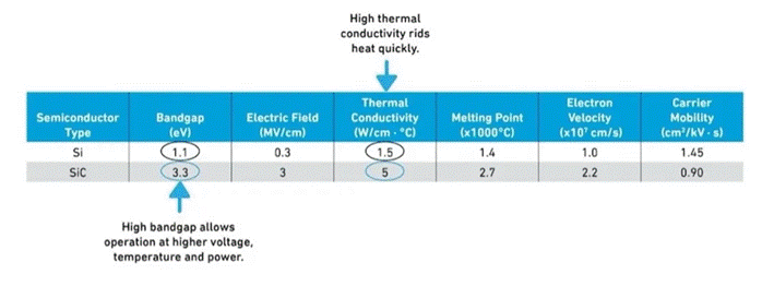
(Photo credit: Qorvo)
• SiC breakdown voltage is higher, which means thinner devices can support higher voltages.
•SiC devices have a smaller bare metal size and lower parasitic capacitance, as well as lower on-resistance, which can lead to lower switching losses and provide higher efficiency.
• SiC power devices can operate at higher switching frequencies for a given voltage and resistance level, allowing smaller peripheral passive components to be used, reducing the size and cost of the overall system.
• Thanks to excellent thermal performance, SiC devices are able to operate at higher ambient temperatures, helping to simplify cooling system design.
In short, SiC power devices have high voltage blocking capabilities, low on-off losses, low switching losses, and high thermal conductivity, so they can provide higher efficiency, better heat dissipation performance, and higher power density for power electronics applications, helping users break through the performance ceiling of silicon-based devices.
Because of this, many "players" in the power electronics industry are actively exploring the use of SiC technology to replace silicon-based processes, developing a series of power devices, such as BJT, JFET, MOSFET and IGBT. However, the development of SiC commercial devices is a new topic after all, and a lot of homework needs to be done to achieve the silky upgrade from Si to SiC technology.
There are two key points to achieve this technology iteration: one is to reduce the cost, including the cost of the SiC device itself, and the supporting cost in the application development (such as gate driver); On the other hand, it is necessary to give full play to the advantages of SiC according to the target application, develop differentiated products, and provide greater choice for developers.
A new path to SiC technology
At present, in the process of moving towards SiC technology, SiC MOSFET is a "must option" for many manufacturers, because compared with Si MOSFET, it has the outstanding advantages of high voltage resistance, low on-resistance, high switching frequency, and a very wide range of applications.
However, as mentioned above, SiC MOSFET is not the only option to "upgrade from Si to SiC silky slip", Qorvo chose to start with SiC JFET to explore a different new path.
As we all know, JFET is a normally open transistor, is the use of gate PN junction depletion layer to achieve switching control, while the normal state of single polarity conduction, compared with MOSFET, such devices have good high frequency characteristics, and because no gate oxygen layer is required, its reliability is better, the on-resistance will be smaller.
But there is a challenge when developing SiC JFET: Compared with SiC MOSFETs, normally open SiC JFTS need to apply a large negative bias when the device is blocked, so that the channel area is completely cut off, so it is not compatible with the drive circuit of existing power devices (such as MOSFET, IGBT, etc.), which will undoubtedly increase the difficulty of the application development of SiC JFET devices.
To this end, Qorvo adopted an ingenious approach - based on a unique "common source common gate structure" circuit configuration, a normally open SiC JFET device and a silicon MOSFET vertical cascade, co-packaging, to form an integrated normally closed SiC FET device. The driver of the device can be compatible with the silica-based MOSFET/IGBT device, which solves the key problem in this SiC technology upgrade.
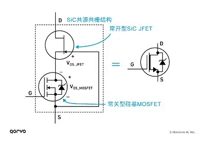
(Photo credit: Qorvo)
From Figure 3, we can further understand the differentiating advantages of Qorvo SiC FETs compared to SiC MOSFETs.
First, there is no gate oxide layer of SiC MOSFETs in Qorvo's SiC JFETs, thus eliminating channel resistance and making the bare chip size more compact, which means that Qorvo SiC FETs provide lower on-resistance (RDS(ON)) for a given chip size. In other words, under the same on-resistance conditions, the Qorvo SiC FET requires a smaller SiC strip size, which allows the device to be used in smaller packaging forms such as TOLL and D2PAK, further strengthening the advantages of SiC device miniaturization.
In addition, Qorvo's SiC FETs also have lower output capacitance compared to SiC MOSFETs, which enables them to operate at faster switching speeds at low load currents, resulting in shorter capacitor charge delays. The resulting benefit is that the need for larger passive components such as inductors and capacitors is reduced, allowing the end device to achieve smaller volume, lighter weight, lower cost, and achieve higher power density.
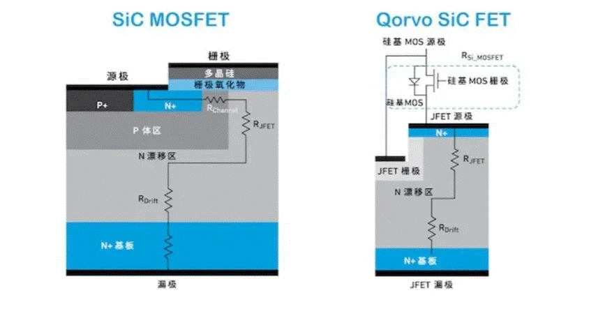
(Photo credit: Qorvo)
• Standard silicon gate drivers are available, which makes the technology transition from Si to SiC smoother and also provides engineers with greater design flexibility.
• Lower drain-source on-resistance RDS(ON) for the same chip area, further improving system efficiency.
• Lower capacitance allows for faster switching speeds and higher operating frequencies, reducing the need for large passive components.
• Higher voltage classes (1,200V or higher) are available with higher operating frequencies than silicon-based IGBTs of the same class.
Rich SiC FET product portfolio
The UF3C series is a representative product in Qorvo's high performance SiC FETs with an ultra-low gate charge, ideal for switching inductive loads and applications requiring standard gate drives. Compatible with standard gate drivers, the UF3C series SiC FETs enable true "silk-smooth leveling" of silicon-based IGBTs, FETs, MOSFETs or hyperjunction devices.
The series of SiC FETs is available in 650V, 1,200V and 1,700V withstand voltage versions, as well as package options such as D2PAK-3, D2PAK-7, D2PAK-7L, TO-247-3L, TO-247-4L and TO-220-3L. It can be widely used in electric vehicle charging, photovoltaic inverters, switching mode power supplies, power factor correction modules, motor drivers and induction heating and other power electronic systems.
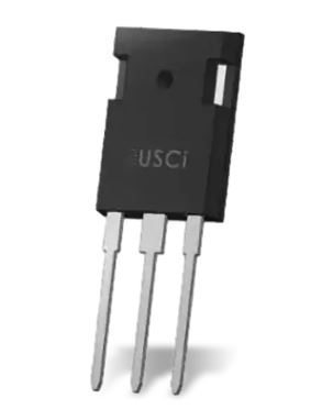
(Photo credit: Qorvo)
UJ Series
The slow switching speed makes it ideal for replacing existing non-Kelvin package designs such as TO247-3L, D2PAK3L, etc.
UF series
Faster switching speed for high switching frequency, high efficiency and high power density applications.
UG series
There are two gate pins, one for SiC JFET and one for Si MOSFETs. SiC JFET gate pins enable very wide switching speed controllability. Its target applications are scenarios with very high currents and relatively slow dv/dt (<20V/ns), such as circuit protection.
That is, side-by-side common-source common-gate or stacked common-source common-gate - the letter "C" means that the common-source common-gate structure is side-by-side packaged with Si low-voltage MOSFET and SiC high-voltage JFET; The letter "SC" indicates a common source common gate structure with an Si low voltage MOSFET chip attached to the top of the SiC high voltage JFET chip, hence the name stack chip.
E1B module
Industry standard modular package, pin compatible with many vendor products, suitable for ZVS soft switch applications such as phase-shifted full bridge, LLC, etc.
Summary of this article
In the field of power semiconductors, the transition from Si to SiC technology has been the general trend, and everyone has formed a consensus. However, how to make this process more "silky" and get as much benefit from SiC as possible with as little cost as possible - for this problem, different manufacturers have their own different high tips.
In this regard, the solution given by Qorvo is very unique and ingenious, through the common source and common gate architecture of Si MOSFET + SiC JFET, it makes up for the performance shortcomings of SiC MOSFET, and is compatible with the gate driver of standard silicon-based devices, which can effectively accelerate the process of SiC device design import.
From Si to SiC, how to silky upgrade? The answer you want is right here
Qorvo UF3C SiC FET For more details
免责声明: 本文章转自其它平台,并不代表本站观点及立场。若有侵权或异议,请联系我们删除。谢谢! Disclaimer: This article is reproduced from other platforms and does not represent the views or positions of this website. If there is any infringement or objection, please contact us to delete it. thank you! |

WeChat Official Account

WeChat Service
 Email
Email QQ
QQ 13823761625
