
DC/DC converters are being designed faster and faster to reduce the size of output capacitors and inductors to save board space. Because of this, there are more and more DC/DC converters on the market that operate at high input voltages to provide line voltage transient protection, and the lower duty cycle makes it difficult to achieve lower voltages at faster frequencies. Many power integrated circuit manufacturers (ics) are actively marketing high-frequency DC/DC converters, claiming that they can reduce board space. DC/DC converters operating at 1MHz or 2MHz May seem like a good idea, but switching frequency has an impact on power systems far beyond volume and efficiency. Several design examples are presented to illustrate some of the benefits and challenges of switching at high frequencies.
Application selection
To illustrate the tradeoff process using high switching frequencies, we designed three independent power supplies operating at 100, 300, and 750 kHz. In all three designs, the input voltage is 48V, the output voltage is 5V, and the output current is 1A. These requirements are often used to power a 5-V logic USB, or an intermediate frequency universal 5-V bus used by other DC/DC converters, such as low voltage drop regulators. To establish some design limitations, the selected allowable ripple voltage needs to be 50mV, which is about 1% of the output voltage; Also choose to use A peak-to-peak inductor current of 0.5 A. The Texas Instruments TPS54160 is a 2.5-MHz, 60-V, 1.5-A buck DC/DC converter with integrated MOSFETs used as a voltage regulator in all designs. The TPS54160 features externally compensated and fast programmable frequencies for some industrial applications with high input voltages.
Inductance and capacitance selection
Select the inductance and capacitance for each case according to the following four simplified formulas:
Inductance selection

Can be rewritten as:
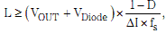
Where D (duty cycle) =5 V/48 V=0.104, and △I = 0.5 A peak-to-peak.
Capacitance selection
I= C x dv/dt (2a)
Can be rewritten as:
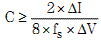
Where △I = 0.5A peak-to-peak, and △V=50 mV.
For equation 2b, we assume that the equivalent series resistance (ESR) of the selected capacitor is negligible, as is the case with ceramic capacitors. We chose ceramic capacitors for all three designs due to their low resistance and small size. The multiplier 2 for the molecule of equation 2b shows a decrease in DC bias-dependent capacitance because this effect is not stated in the data sheets for most ceramic capacitors.
FIG. 1 Reference diagram of TPS54160
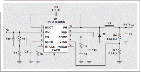
The circuit shown in Figure 1 is used to evaluate the performance of each design on the bench. Some components that do not have values in the diagram are components that have been modified in the design. The output filter consists of L1 and C2. The component values for all three designs are listed in Table 1 and are selected based on the results of equations 1a to 2b. Note that the DC resistance of each inductor decreases with increasing frequency. This is because fewer turns require a shorter length of copper. We designed an error amplifier compensation component individually for each switching frequency. The calculation method of selecting compensation value is beyond the scope of this article.
Minimum "on" time
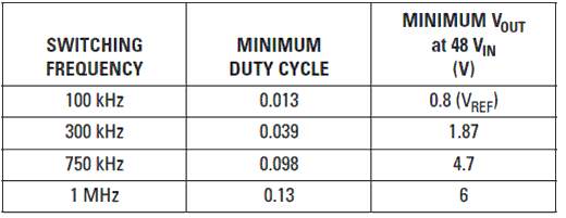
The minimum controllable "on-on" time limit is a characteristic of DC/DC converter ics, which is the narrowest reachable pulse width of a pulse width modulation (PWM) circuit. In buck converters, the percentage of time the power MOSFET is on during the switching cycle is called the duty cycle, which is equal to the ratio of the output voltage to the input voltage. When using the TPS54160 converter, the duty cycle is 0.104 (4 V/48 V), while the minimum "on" time listed in the data table is 130 ns. The controllable pulse width limit produces a minimum reachable duty cycle, and we can easily calculate the size of this duty cycle by multiplying the minimum "on" time by the switching frequency. Once we know the minimum duty cycle, we can calculate the minimum reachable output voltage by multiplying VIN by the minimum duty cycle. The minimum output voltage is also limited by the converter reference voltage, which is 0.8V with the TPS54160.
In this example, we can generate a 5-V output voltage with a 750-kHz switching frequency (see Table 2). However, if this frequency is 1 MHz, the lowest possible output voltage is limited to about 6V; Otherwise, the DC/DC converter will skip the pulse. The alternative is to reduce the input voltage or frequency. Before selecting a switching frequency, it is a good idea to check the DC/DC converter data sheet for a guaranteed minimum controllable "on" time.
Pulse jump
A pulse jump occurs when the DC/DC converter cannot clear the gate drive pulse fast enough to maintain the ideal duty cycle. The power supply will try to adjust the output voltage, but the ripple voltage will increase due to pulses that are farther away. Because of the pulse jump, the output ripple will present a subharmonic component, which may cause noise problems. The current limiting circuit may also no longer function properly because the IC may not respond to large current spikes. In some cases, if the controller is not working properly, the control loop may be unstable.
Efficiency and power consumption
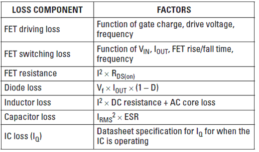
The efficiency of a DC/DC converter is one of the most important attributes to consider when designing a power supply. Low efficiency translates into high power consumption, and it is necessary to use a separate heat sink or more copper on the printed circuit board (PCB) to handle these power consumption. Power consumption also puts higher requirements on upstream power supply devices. As shown in Table 3, power consumption has several components.
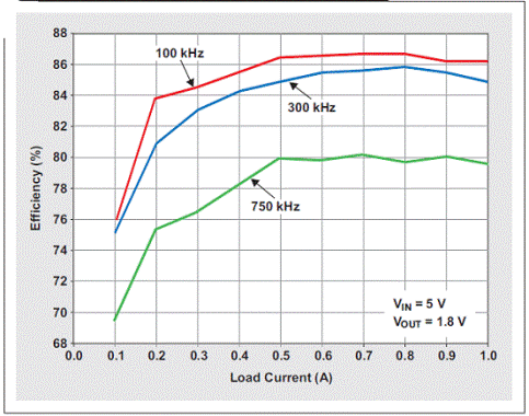
The important loss components of the three examples come from the FET drive loss, FET switching loss, and inductance loss. The FET resistance and IC loss are consistent because the same IC is used in all three designs. Since ceramic capacitors with low ESR are selected in all examples, the capacitance loss is negligible. To show the effect of the high-frequency switch, we measured the efficiency of each example and showed it in Figure 2. The figure clearly shows that the efficiency decreases as the switching frequency increases. To improve efficiency at all frequencies, you need to find a DC/DC converter with low leak-to-source "on-on" resistance, low gate charge, or low static current specifications at full load. Or find some capacitors and inductors with lower equivalent resistance.
Table 1 Selection of capacitors and inductors for three example power supply designs
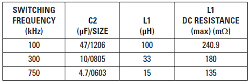
Table 2 Minimum output voltage for the minimum "on" time of 130-ns
Table 3 Power consumption components
Figure 2 Efficiency of TPS54160 at three example frequencies
Component size
Table 4 lists the total board area for the three design requirements, as well as the pad area for capacitors and inductors. The recommended pad area for the capacitor or inductor is slightly larger than the individual component itself and is used in all three design examples. Add the area occupied by each component (which includes the pad size of the IC, filter, and all other small resistors and capacitors) and multiply the resulting result by 2 (taking into account the spacing of the components) to get the total area. There is a total area savings of nearly 250 mm2 between the 100-kHz and 750-kHz designs, resulting in a 50% reduction in filter volume and a 55% reduction in board space occupancy. However, there is a law of diminishing returns because capacitance and inductance values cannot be reduced to zero! In other words, pushing up the frequency doesn't always reduce the overall size, because you can't always buy mass-produced inductors and capacitors in these sizes on the market. Note that 33-µH and 15-µH inductors occupy the same area. This possibility exists because the 33-µH inductor is 3.5 mm in height, while the 15-µH inductor is only 2.4 mm higher. The point we want to make through thes
Table 4 Component dimensions and total area requirements
Transient response
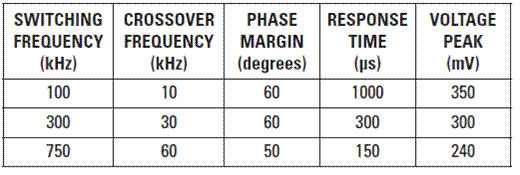
Transient response is a good indicator of power supply performance level. We use the Baud chart for each power supply to show how high switching frequencies compare (see Figure 3). As shown in the figure, the phase margin of each power supply is between 45° and 55°, which indicates that the transient response is well suppressed. The crossover frequency is about 1/8 of the switching frequency. When using fast-switching DC/DC converters, designers should ensure that the power IC error amplifier has sufficient bandwidth to support high crossover frequencies. The unit gain bandwidth of the TPS54160 error amplifier is generally 2.7 MHz. Table 5 shows the actual transient response time and the correlation values of the voltage peak overshoot. The higher the switching frequency, the lower the overshoot value, because of the wider bandwidth.
Table 5 Transient response
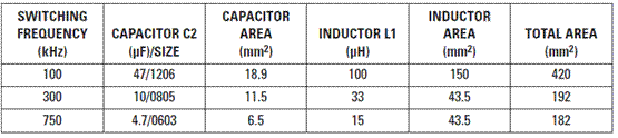
Table 6 Ratio of jitter to "on" time for small duty cycle
Jitter consideration
At high conversion ratios and higher frequencies, there are noise problems. When selecting a certain high switching frequency, designers should consider jitter and the minimum "on" time of the DC/DC converter. When the duty cycle is small, the jitter noise is a larger percentage of the switching pulse. Table 6 shows the ratio of jitter to "on" time for the 48-V to 5-V conversion ratio. We assume that there is a 0.5-V diode voltage drop and 20-ns jitter at this phase node.
conclusion
When designing high frequency switching converters, there are many trade-offs. Some of the advantages described in this article include smaller size, faster transient response, and smaller voltage overshoot/undershoot. The cost of these advantages is low efficiency and more heat dissipation. However, there are also many pitfalls in the process of pushing performance limits, such as pulse jumps and noise problems. Before selecting a wide input voltage DC/DC converter for high frequency applications, we should first review the data sheet provided by the manufacturer to understand some important specifications, such as: minimum "on" time, error amplifier gain bandwidth, FET resistance, and FET switching loss. An IC that works well under these specifications is expensive, but worth its price; It is easier to use when designers are worried about how to deal with a difficult design problem.
免责声明: 本文章转自其它平台,并不代表本站观点及立场。若有侵权或异议,请联系我们删除。谢谢! Disclaimer: This article is reproduced from other platforms and does not represent the views or positions of this website. If there is any infringement or objection, please contact us to delete it. thank you! |

WeChat Official Account

WeChat Service
 Email
Email QQ
QQ 13823761625
