
"Electronic equipment changes with each passing day, promote the continuous development of power technology, electronic equipment for safety and energy saving, portable and easy to use and performance of common requirements, feedback to the power chip, chip developers need to develop higher efficiency, lower power consumption, more intelligent green power chip, The goal of achieving higher power density, longer battery life, lower EMI interference, better power supply and signal integrity, and safety at high voltage is driving continuous innovation among power chip developers.
As an essential part of the electronic system, the power module is the most common, and it is also one of the parts that test the skills of hardware engineers. The power module is a subsystem of electrical energy conversion, distribution, control and monitoring in the electronic system. The power consumption, performance, cost and volume of the entire electronic system are directly related to the design of the power module. Modern large electronic systems are developing towards high integration, high speed, high gain and high reliability. The small interference on the power supply will affect the performance of the electronic equipment, which requires the design of a power module with low noise and strong anti-ripple ability. In portable devices, more and more battery power supply, which puts high requirements on battery life, which usually corresponds to the extreme requirements of its power module efficiency, high reliability and low static current.
In short, the design of the power module is the basis of the performance of the electronic system, and only after the design of the power module of the system is done, can we have the opportunity to pursue performance and realize all the functions of the system stably. The power module design is extremely important is how to choose the right chip and technical solution. Usually, according to the situation of each branch in the power module, determine the input and output voltage difference, and then according to the application requirements, under the constraints of efficiency indicators, heat dissipation limits, noise requirements, system complexity and cost, the most suitable power chip can be selected, and then according to the selected power chip to achieve the corresponding power conversion and distribution functions.
According to the application scenario, power modules can be divided into AC to DC (AC-DC) conversion power modules and DC-DC (DC-DC) conversion power modules. Ac-dc power modules are usually used for devices that directly use mains power, while DC-DC power modules can only connect to DC power supplies and then divide or boost the voltage based on the DC power input. Supply the required voltage and current to each module of the system.
According to the working principle, the power supply chip can be divided into linear power supply chip and switching power supply chip. Linear power supply is also known as Low Drop Out Regulator (LDO) chip, the principle is through the transistor voltage drop to adjust the output voltage, can only achieve step-down output, can not achieve boost output, compared with the switching power supply chip, LDO usually has small size, low noise, easy to use and other characteristics.
The switching power supply chip uses pulse width modulation (PWM) mode to work, can achieve the boost and drop output, and has high efficiency and low power consumption, but because it uses PWM mode to work, it will produce electromagnetic interference (EMI), so the noise is usually larger than the corresponding LDO.
According to the implementation method, the switching power supply can be divided into two categories, that is, the inductive DC-DC power supply chip and the DC-DC converter based on the switching capacitor (that is, the charge pump DC-DC chip). Charge pump DC-DC chip uses capacitor as switch and energy storage component, compared with inductive DC-DC power chip, it has the advantages of high efficiency, small size, low static current, wide output voltage regulation range, low Vmin, low noise and low EMI, and capacitor is easier to integrate than inductor, so charge pump power chip can achieve higher integration. In low-power applications, charge pump DC-DC switching power supply chip has great advantages, but charge pump power supply chip is not suitable for high-voltage, high-power scenarios, so in high-power applications, inductive DC-DC power supply chip is still dominant.
In complex systems with large chips such as high-performance processors and large FPGas, a combination of switching power supply and LDO is usually required because the current consumption can reach several amps to tens of amps. An analog circuit that is susceptible to interference in a complex system, usually powered by an LDO chip; And the digital part because of the large current and therefore high efficiency requirements, and the digital circuit itself is more anti-interference, so it is more suitable for switching power supply. The combination of switching power supply, LDO and various protection devices and passive components builds the power distribution system of complex systems.
In short, LDO and switching power supply are the core of power modules in all electronic devices, and the development of electronic systems has also put forward higher requirements for power chips, and R&D personnel continue to try to update the manufacturing process, packaging technology and circuit topology to achieve more extreme performance or other indicators such as volume and cost. Below we will look at the development trend of power chips to see how to choose the right power chip.
Lower static current - lower loss
Nearly 2 billion mobile phones (including smart phones and feature phones) are shipped each year, and more than 100 million laptops are shipped each year, and with the development of Internet of Things technology, more and more battery-powered devices are connected to the network, and these devices typically work for a short period of activation, relatively long hibernation, and usually need to work for a whole year, or even three to five years, without replacing the battery. Such applications put very high requirements on the power chip, which requires very low static current to maintain the power efficiency of light load or no load, to meet the requirements of the device for long battery life, and to meet the requirements of the system for power supply capacity under heavy load.
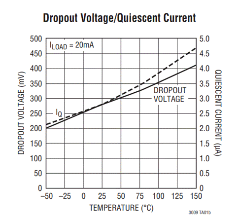
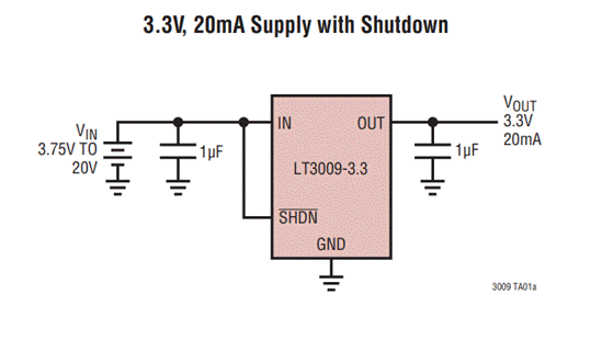
The LT3009 from Analog Devices (ADI) is an LDO chip that can meet both microamps (uA) static operating current and 20 milliamps (mA) large drive capability. Specifically, the LT3009 has a no-load static current of 3uA and can deliver 20mA output current at 280mV differential pressure (input/output) with input voltage range of 1.6V to 20V and output voltage range of 0.6V to 19.5V. In addition, the LT3009 only requires 1uF capacitance to ensure the stability and instantaneous response of the output power supply, and the internal integration of current limiting, temperature limiting, battery protection and reverse current protection and other protection functions can effectively ensure the safety of portable devices.
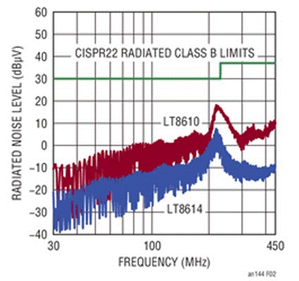
EMI (electromagnetic interference) reduction is mainly for the Switch power chip (Switch Regulator). Because the switching power supply chip works in the pulse width modulation state, the switching frequency is mostly several hundred KHz to several MHz, or even higher, so the switching power supply itself is the source of interference. If the switching power supply circuit is not ideally set at the time of implementation, it will aggravate the electromagnetic interference emitted by it, and sometimes the electromagnetic compatibility test of the device can not pass, possibly because the switching power supply part is not handled well.
The method of reducing EMI on the equipment circuit board is mainly shielded or filtered (the circuit can be modified), reducing the switching waveform rise slope, if the chip has the spread frequency function, it can also play the frequency function, and modify the PCB wiring. In general, methods of optimizing EMI at the board level have costs, such as increasing costs or affecting power performance. The best solution is that the switching power supply chip itself fully considers the electromagnetic interference problem when the board is implemented, and the EMI problem is solved at the chip level, the cost is low, and the system performance will not be affected.
ADI's Silent Switcher technology significantly improves the EMI performance of switching power supplies at the chip level, so that EMI can be effectively reduced without affecting the performance of the power supply, and without adding external components, which is a simple and efficient low-cost solution.
In addition to EMI, in applications such as medical electronics, precision instrumentation, high-precision power supplies and communication infrastructure, the noise and power ripple rejection ratio (PSRR) requirements for the power chip itself are also very high, because in these applications, there are often sensitive circuit modules such as ADC, DAC circuits, precision amplifiers, high-frequency oscillators, clocks, and PLLS. If the power supply is not clean, the performance of these sensitive circuits will be greatly affected, because the sensitive circuit has high requirements for noise, so usually the module can only be powered by the LDO chip with better noise suppression. With the changes in market applications, sensitive precision circuit technology continues to develop, and precision LDO power chips are continuously promoted in the direction of lower noise and higher accuracy.
LDO noise comes from two parts, internal noise and external noise. The internal noise is mainly thermal noise and 1/f noise, which are related to LDO design and semiconductor process. There are many sources of external noise, the most common being the noise of the LDO input power supply (usually powered by the output of the switching power supply chip). Because the LDO has high gain, which ensures good line and load tuning performance, it is able to attenuate noise and ripple from the input power supply, which is the power ripple rejection ratio of the LDO, and its PSRR decreases as the frequency increases due to the limited bandwidth of the LDO. Noise outside the LDO bandwidth cannot be attenuated by the LDO itself and needs to be reduced by a passive filter.
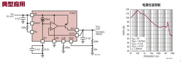
The LT3042 from ADI is an ultra-low noise, ultra-high PSRR architecture LDO chip for sensitive circuit applications. The LT3042 has an RMS noise of only 0.8uV (RMS value) at 10Hz to 100kHz, a point noise of only 2nV/Hz at 10kHz, and a PSRR of 79dB at 1MHz. Figure 8 below shows the typical application circuit and PSRR parameters of the LT3042.
Better isolation
The above are all low-power applications, and in high-power applications, the power chip is also indispensable. High-power applications have an additional requirement compared to low-power applications, namely isolation. The function of isolation is to cut off the direct circuit between the high current and high voltage module and the small current and low voltage module in the electronic system, and transfer the control signal through the coupling method to achieve the protection of the operator and the low voltage circuit module, and reduce the interference of the high voltage and high current module to the low voltage circuit part.
Optical coupling isolation is a more traditional isolation method, but it has many disadvantages, such as easy aging, slow speed and high power consumption. However, before the advent of digital isolation technology, optocoupler was an extremely suitable isolation scheme. In the late 1990s, digital isolation technology began to be industrialized, because of its size, speed, power consumption, ease of use and reliability has a huge advantage that optical couplers can not match, so it was widely praised by the market.
ADI is one of the leaders in digital isolation technology, having shipped more than 3 billion isolation channels with its iCoupler digital isolation chip and uModule BGA digital isolation technology. The ADUM6421A is a DC/DC switching power supply chip that integrates four iCoupler on-off key control (OOK) digital isolation channels and iCoupler chip-level isoPower transformer technology. Enables small integrated, enhanced isolated signal and power solutions in 500mW isolated power supplies.
The ADUM6421A common-mode transient immunity (CMTI) is up to 100kV/µs, meeting enhanced isolation requirements, and is optimized for EMI to meet CISPR 32/EN550 32 Class B emission limits at full load on a 2-layer PCB.
miniaturization
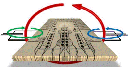
Miniaturization is one of the main directions of the current development of power module technology, miniaturization can reduce the occupied PCB area, reduce the weight of the equipment, and facilitate the equipment to integrate more functions, and the miniaturization of the power chip or module is of great significance for hardware engineers. But miniaturization means high power density, that is, the same volume provides more power output, which requires the power chip to have higher conversion efficiency and better heat dissipation performance.
The developers meet the demand for power miniaturization by applying four directions of technology. First, better semiconductor processes to reduce the heat emitted by the chips themselves; Secondly, innovative circuit topology and structure are adopted to reduce the requirements for external passive devices, so that small passive devices can meet the system requirements. Third, innovative packaging technology to enhance the power chip heat dissipation capability; Finally, parasitic parameters and chip size are reduced through heterogeneous integration.
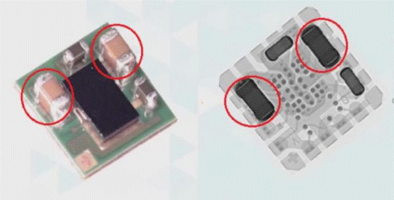
ADI has a strong presence in all of these directions. A typical case is the improvement of low voltage and high current FPGA chip power supply scheme. In 2010, ADI required 12 LTM4601 chips for FPgas that required 100A current. By 2012, four LTM4620 pieces in parallel can output 100A current; The LTM4630, launched in 2014, only needs three pieces in parallel to output 100A current. Launched in 2016, the LTM4650 only needs 2 pieces to supply 100 amps of current. But that's not the point, ADI has launched the LTM4700 to achieve a single chip power supply of 100A.
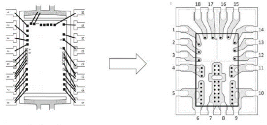
The evolution of the LTM series is particularly obvious in the evolution of packaging technology, from ordinary plastic packaging, to the addition of metal cooling substrate, and then to the development of its own Component on Package (CoP). CoP This is a three-dimensional packaging technology, which puts the inductor outside the high-power power chip above the chip through the packaging technology, exposing it as a heat sink in the air flow, so that it does not occupy the PCB area, but also improves the heat dissipation performance, so that the power density can be improved.
Sum up
Electronic equipment changes with each passing day, promote the continuous development of power technology, electronic equipment for safety and energy saving, portable and easy to use and performance of common requirements, feedback to the power chip, chip developers need to develop higher efficiency, lower power consumption, more intelligent green power chip, The goal of achieving higher power density, longer battery life, lower EMI interference, better power supply and signal integrity, and safety at high voltage is driving continuous innovation among power chip developers. In turn, the continuous innovation of power chip technology also gives electronic equipment research and development personnel more incentives and resources, and gives engineers more choices when doing power supply design, so that these new technologies can be applied to the extreme.
免责声明: 本文章转自其它平台,并不代表本站观点及立场。若有侵权或异议,请联系我们删除。谢谢! Disclaimer: This article is reproduced from other platforms and does not represent the views or positions of this website. If there is any infringement or objection, please contact us to delete it. thank you! |

WeChat Official Account

WeChat Service
 Email
Email QQ
QQ 13823761625
