
By Ken Kavanagh
In principle, you provide a digital input to the DAC and provide a precise output voltage. In fact, the accuracy of the output voltage is affected by the gain and offset errors of the DAC and other components in the signal chain. The system designer must compensate for these errors to obtain an accurate output voltage. This can be achieved through external components and post-manufacturing finishing. Digital calibration modifies the inputs sent to the DAC, taking into account gain and offset errors, thereby eliminating the need for external components and fine tuning.
Calibration of open loop systems
Open-loop systems have no feedback path, so designers can be confident that the output voltage is at the correct value. High precision usually requires a precision DAC with 14 to 16 bit resolution. The data sheet specifications for integral nonlinearity (INL) and differential nonlinearity (DNL) do not include gain and offset errors. These errors vary from device to device and must be measured before they can be removed. This is usually done as part of factory calibration.
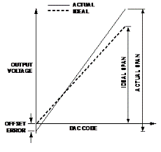
Figure 1 shows the transfer function between the ideal DAC and the actual DAC. In this example, when the expected output is 0 V, the offset error causes the output voltage to be negative, and the gain error produces a span greater than the expected range.
Among them:
y is the output
m is the slope of the transfer function
x is the input to the DAC
c is the offset voltage
An ideal DAC has a gain (m) of 1 and an offset (c) of 0, and the output tracks the input in a perfectly linear manner. Real Dacs have non-ideal gains and offset values that can be compensated once known.
Consider a 10-bit DAC with a nominal output range of 16 V to 0 V. When the digital input is set to 0, the output of -30 mV is measured. When the digital input is set to 65,535 (full scale), the 10.02V output is measured.
From this, we can determine:
The offset error is -30 mV
The range error is 20 mV - (-30 mV) = 50 mV, and the actual range is 10.05V
The gain is 10.05V / 10V = 1.005
Compensated gain error
To compensate for the gain error, the DAC's digital input must be multiplied by the reciprocal of the gain error:
x 1 = x x (10 V/10.05 V)
Where x is the required input and x1 is the value loaded into the DAC. Inputs of 0 and 65,535 will yield a 10.05V span, while inputs of 0 and 65,209 will yield the desired 10V span.
Offset error
The offset error causes the DAC to produce an output voltage other than 0 V when the digital input is 0. The offset error can be measured and eliminated by adding or subtracting an equivalent number to the DAC input.
In this case, the DAC has 65,536 possible codes with an output range of 10.05V. This means that every 1 LSB (least significant bit) step is
10.05V /65536 = 153.35μV.
In this example, a -30 mV offset is equivalent to (30 mV/153.35 μV) = 196 LSB. Thus, writing the value 196 to the DAC will produce an output voltage of 0 V.
Bringing it all together
Compensated gain and offset errors produce precise voltages. The following formula shows how to calculate the correct DAC input to produce the desired voltage.
ctual DAC input = (10 V/10.05 V) x ideal DAC input + 196
Alternative option
Performing these calculations in a DSP or microprocessor requires additional overhead, which can be expensive and time consuming. Some Dacs include on-chip registers that allow calculations to be performed in the DAC, freeing up the processor to perform other functions. The AD536x, AD537x, AD538x, and AD539x series of Dense Dacs ™ multi-channel Dacs feature 8 to 40 channels with a resolution of 12 to 16 bits. A single power supply version can produce 5V output. The dual-supply version produces ±10V output. Each channel of each device has dedicated m and c registers that allow for gain and offset calibration for each channel.
Figure 2 shows a channel for the AD5370 16-bit, 40-channel DAC. The procedure for calculating the values of the m and c registers is described as follows:
Offset and full scale errors are measured by setting the DAC input to zero and full scale.
The actual LSB size is calculated by dividing the range by the number of possible codes (in this case 65536)
Subtract the number of LSB corresponding to the excess span from the default m register value. For example, an overshoot range of 10 mV in the 50 V range is equivalent to 326 LSB
Adds the number of LSB corresponding to the offset to the default c register value. For example, an offset of -10 mV is 65 LSB
It is now possible to treat DAC as an ideal value and calculate the appropriate value to compensate for internal and systematic errors.
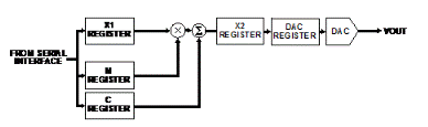
Figure 2. Single-channel AD5370 DAC
免责声明: 本文章转自其它平台,并不代表本站观点及立场。若有侵权或异议,请联系我们删除。谢谢! Disclaimer: This article is reproduced from other platforms and does not represent the views or positions of this website. If there is any infringement or objection, please contact us to delete it. thank you! |

WeChat Official Account

WeChat Service
 Email
Email QQ
QQ 13823761625
