
The power factor correction (PFC) market is primarily influenced by global regulations related to harmonic distortion reduction. Europe's EN61000-3-2 is one of the basic provisions of the AC and DC power supply market, and similar standards exist in the United Kingdom, Japan and China. En 61000-3-2 specifies harmonics standards for all off-line devices with power consumption exceeding 75W. Since there are no regulations governing PFCS in North America, energy savings and space/cost considerations become additional drivers for the mandatory use of PFCS in consumer products, computers, and communications.
There are two general modes of active PFCS: discontinuous current mode (DCM) using triangular and trapezoidal current waveforms and continuous current mode (CCM). DCM mode is generally used for applications with output power between 75W and 300W; CCM mode is used for applications with output power greater than 300W. When the output power exceeds 250W, the PFC is cost-effective because other aspects (such as efficiency) are compensated for, so no additional cost is actually added.
Active PFC is a requirement for server System architecture (SSI) conformance: the power supply module should have a universal power input with active power factor correction, which can reduce harmonics and comply with EN61000-3-2 and JEIDA MITI standards. This requires high power density applications to be able to provide a wide input voltage range (85 to 265V), which puts special requirements on the semiconductors used in PFC-level circuits.
At 85V AC voltage input, there must be a minimum Rdson, because the conducted heat loss is inversely proportional to the third power of the input voltage. The high frequency operation of this MOSFET tube can significantly reduce boost suppression. Therefore, the fast switching characteristics of the transistor are necessary. The boost diode should have fast switching, low Vf and low Qrr characteristics. In order to reduce the peak current pressure of the MOSFETs when switched on, a low Qrr is a must. Without this feature, the boost MOSFETs will increase temperature and Rdson, resulting in more power loss, which reduces efficiency. In high power density applications, efficiency is a key factor in achieving smaller volumes (30W/cm3 inches) and reducing the size of passive devices. Therefore, a high switching frequency is essential.
In order to design CCM PFCS with optimal efficiency and form factor, the boost diode must also have the following characteristics: short reverse recovery and forward recovery time; Minimum stored charge Q; Low leakage current and minimal switching loss. Overvoltage and surge current capabilities are important to handle surges and overcurrents caused by startup and AC fall in PFC. These properties can only be achieved with silicon carbide Schottky diodes (SiC Schottky diodes).
Due to the lack of forward and reverse recovery charges in SiC Schottky diodes, smaller boost MOSFETs can be used. In addition to the cost reduction, the device temperature is also reduced, which makes the SMPS more reliable.
Since the switching behavior of SiC Schottky diodes is independent of forward current (Iload), switching speed (di/dt), and temperature, this diode is easy to use in design. The use of SiC Schottky diodes in the design enables the maximum switching operating frequency (up to 1MHz), allowing the use of smaller passive devices.
Minimum switching losses and low Vf enable the use of smaller radiators or fans. In addition, because of the positive temperature coefficient, SiC Schottky diodes can be conveniently placed in parallel.
thinQ! 2G towards the ideal high voltage diode
New generation IFX SiC Schottky diodes (thinQ! 2G) combines a common SiC Schottky diode with a bipolar pn structure, resulting in very high inrush current tolerance and stable overvoltage characteristics.
Figure 1 compares the SiC Schottky diode structure with the combined pn Schottky diode concept. The p region is optimized for emitter efficiency and conductivity, so it can be used as a bypass channel for inrush current when the forward voltage exceeds 4V.

thinQ! 2G offers improved surge current functionality that allows design for average current conditions in the application, meaning that most surges and overcurrents caused by startup and AC fall can be handled well. Figure 2 shows that in normal working condition, thinQ! 2G behaves like a normal Schottky diode with zero reverse recovery charge, and its forward characteristics are similar to bipolar pn diodes in high current states, which can significantly reduce power loss.

Tests for practical applications (6A IFX 1st generation SiC Schottky diodes, PFC, wide range) confirm these improvements: 6A 1st generation SiC Schottky diodes are sufficient to handle the inrush current at start-up, with junction temperatures up to 50 ° C. This situation is very close to the thermal runaway caused by Schottky properties, as shown in Figure 2. In general, smaller diodes can be used.
The new 4A thinQ! 2G can better handle startup conditions in the same application. The temperature only rose to 35℃. Due to the bipolar characteristics, no runaway heat is generated when the maximum junction temperature is reached. thinQ designed to work in normal conditions! 2G has enough margin to handle exceptions.
Stable overvoltage characteristics
In addition to the improved inrush current function, the thinQ incorporates the pn Schottky concept. 2G can withstand actual avalanche current breakdown conditions. This is not possible with any other SiC Schottky diode on the market today. This is due to the low resistivity and the design of the p island incorporated in the Schottky structure, which ensures that the avalanche starts before the electric field at the Schottky junction reaches destructive values (Figure 3).
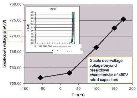
During the transient change in the PFC stage, the overvoltage can be broken down by a large capacitor of about 500 to 550V (for the commonly used 450V large capacitor) Zener. Under these stress conditions, thinQ! 2G protects against dangerous overpressure behavior. This improved overvoltage and surge current capability allows diode pressure to be reduced and applications to be more reliable.
SiC Schottky Diodes - a solution for all power supply conditions
Using silicon carbide with unique properties as the device material, booster diodes with close to ideal functional characteristics can be manufactured and suitable for various power levels in PFC applications. SiC Schottky diodes have no reverse recovery charge, reverse characteristics independent of switching speed, temperature and forward current, and reduce power losses in PFC applications. This is especially important for servers and high-end PC power supplies, as the requirement for efficiency gains becomes increasingly important, especially when it comes to meeting regulatory requirements such as the 80plus.
Increased efficiency through the use of SiC diodes that provide the lowest switching losses is commonly used in systems such as UPS and solar inverters, where each loss reduction directly results in a good return. In view of the increasing efficiency goal, we hope that the application of silicon carbide diodes can be moved to a lower power level: using thinQ! 2G can meet more applications that require higher ambient temperatures, higher device temperatures, and higher reliability.
免责声明: 本文章转自其它平台,并不代表本站观点及立场。若有侵权或异议,请联系我们删除。谢谢! Disclaimer: This article is reproduced from other platforms and does not represent the views or positions of this website. If there is any infringement or objection, please contact us to delete it. thank you! |

WeChat Official Account

WeChat Service
 Email
Email QQ
QQ 13823761625
