
intro
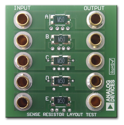
Current detection resistors are available in a variety of shapes and sizes to measure current in many automotive, power control and industrial systems. When using very low values of resistance (a few mΩ or less), the resistance of the solder will occupy a large proportion of the resistance of the detection element, resulting in a significant increase in measurement error. High-precision applications often use 4-pin resistors and Kelvin detection techniques to reduce this error, but these specialized resistors can be expensive. In addition, when measuring high currents, the size and design of the resistance pad play a key role in determining the detection accuracy. This article will describe an alternative that uses a standard low-cost dual pad detection resistor (4 pad layout) for high-precision Kelvin detection. Figure 1 shows a test board used to determine errors due to five different layouts.
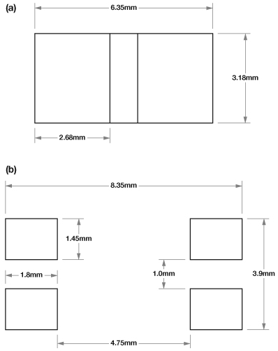
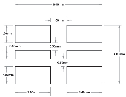
Common current detection resistors in 2512 packages can have resistance values as low as 0.5 mΩ and maximum power consumption as high as 3 W. To demonstrate error under the worst conditions, these tests used a 0.5 mΩ, 3 W resistor with a 1% tolerance (Model: ULRG3-2512-0M50-FLFSLT Manufacturer: Welwyn/TTelectronics) whose dimensions and standard 4-wire package are shown in Figure 2.
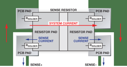
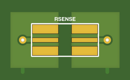
For Kelvin inspection, the standard two-wire sealing pad must be split to provide separate paths for the system current and the inspection current. Figure 3 shows an example of such a layout. The path of the system current is indicated by the red arrow. If a simple double pad layout is used, the total resistance is:

In order to avoid increasing resistance, it is necessary to correctly lay the voltage detection wire to the detection resistance pad. The system current will cause a significant voltage drop at the upper solder joints, but the detection current will cause a negligible voltage drop at the lower solder joints. It can be seen that this pad separation scheme can eliminate the solder joint resistance in the measurement, thereby improving the overall accuracy of the system.
Optimize Kelvin packaging
The layout shown in Figure 3 is a significant improvement over the standard dual pad scheme, but with very low value resistors (0.5 mΩ or less), the effect of the physical location of the detection point on the pad and the symmetry of the current flowing through the resistance becomes more significant. For example, ULRG3-2512-0M50-FLFSL is a solid metal alloy resistor, so the effective resistance is affected for every millimeter of resistance extended along the pad. Using the calibration current, the optimal inspection layout can be determined by comparing the voltage drop under the five customized packages.
Test PCB board
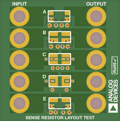
Figure 4 shows the five layout patterns built on the test PCB, labeled A through E. As far as possible, we lay out the lines to test points extending along the test pad at different positions, which are represented as colored dots in the figure. Each resistor is packaged as:
1. Standard 4-wire resistors based on 2512 recommended package (see Figure 2 (b)). The detection point pairs (X and Y) are located on the outer edge and inner edge of the pad (X-axis).
2. Similar to A, but the pad extends inwards longer to better cover the pad area (see Figure 2 (a)). The detection point is located in the center and end of the pad.
3. Use both sides of the pad to provide a more symmetrical system current path. At the same time, move the detection point to a more central position. The detection point is located in the center and end of the pad.
4. Similar to C, only the system current pad is engaged at the most internal point. Only external inspection points are used.
5.A mix of A and B. The system current flows through the wider pad, and the detection current flows through the smaller pad. The detection point is located on the outer edge and the inner edge of the pad.
Test procedure
The test design is shown in Figure 5. Pass A calibration current of 20 A through each resistor while keeping the resistance at 25°C. Within 1 second of loading the current, the resulting differential voltage is measured to prevent the resistance temperature from increasing by more than 1°C. The temperature of each resistor is also monitored to ensure that the test results are measured at 25°C. At A current of 20 A, the ideal voltage drop through a 0.5 mΩ resistor is 10 mV.
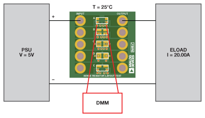
Table 1 lists the data obtained by detecting the pad position as shown in Figure 4.
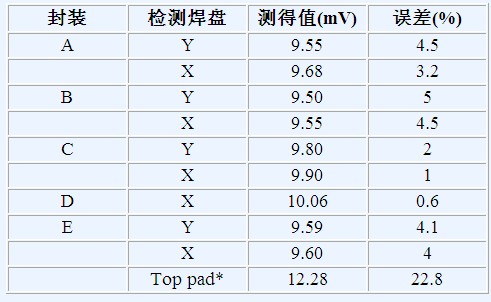
* No Kelvin detection. The voltage through the high current main pad is measured to demonstrate the error associated with the solder resistance.
Observation result
1. Due to the comparability of the results and the resistance deviation are within the tolerance range, the error of package C and D is the least. Package C is preferred because it is less likely to cause problems related to component placement tolerance.
2. In each case, the detection point on the outside of the resistor provides the most accurate results. This suggests that these resistors were designed by the manufacturer based on the overall length of the resistors.
3. Please note that the solder resistance relative error is 22% when Kelvin testing is not used. This corresponds to a solder resistance of about 0.144 mΩ.
4. Package E demonstrates the effect of asymmetrical pad layout. During reflow, the component passes through a large amount of solder before the pad can be welded. This encapsulation should be avoided.
conclusion
According to the results shown above, the best package is C with an expected measurement error of less than 1%. The recommended size for this package is shown in Figure 6.
免责声明: 本文章转自其它平台,并不代表本站观点及立场。若有侵权或异议,请联系我们删除。谢谢! Disclaimer: This article is reproduced from other platforms and does not represent the views or positions of this website. If there is any infringement or objection, please contact us to delete it. thank you! |

WeChat Official Account

WeChat Service
 Email
Email QQ
QQ 13823761625
