
Abstract: Based on the drive and control principle of H bridge of DC motor, this paper analyzes and discusses various problems that may occur in the circuit design process in detail, and puts forward practical solutions. This circuit uses NMOS field effect tube as power output device, designs and realizes a high-power DC motor H-bridge drive circuit, and carries on closed-loop control to 25D60-24A DC motor with rated voltage of 24 volts and rated current of 3.8A. The circuit has strong anti-interference ability and good robustness.
1 Introduction
Dc motor has excellent speed regulation characteristics, smooth speed regulation, convenient, wide speed regulation range, strong overload capacity, can achieve frequent stepless rapid start, braking and reversal, to meet the production process of the automation system of various special operation requirements, so in the field of industrial control, DC motor has been widely used.
Many semiconductor companies have introduced special DC motor driver chips, but most of these chips are only suitable for low-power DC motors, and their integrated chips are expensive for high-power DC motor drivers. Based on this, this paper analyzes and discusses the possible problems in the design of high power DC motor drive circuit, and designs and implements a DC motor drive circuit based on 25D60-24A. The circuit has high driving power and strong anti-interference ability, and has wide application prospect.
2 H bridge power drive circuit design
In the DC motor, GTR collector output type and emitter output drive circuit can be used to drive the motor, but they are irreversible variable speed control, the current can not reverse, no braking ability, can not reverse drive, the motor can only rotate in one direction, so this drive circuit is greatly limited. For reversible variable speed control, H-bridge complementary symmetrical drive circuit is the most widely used. The reversible drive allows the current to reverse, which can realize the four-quadrant operation of the DC motor and effectively realize the positive and reverse control of the motor. The motor speed control mainly has three kinds, adjusting the armature voltage, weakening the excitation flux, changing the armature circuit resistance. The three methods have advantages and disadvantages, changing the armature circuit resistance can only achieve graded speed regulation, weakening the magnetic flux can achieve smooth speed regulation, but the speed range of this method is not large, and it is generally used with variable voltage speed regulation. Therefore, in the DC speed control system, variable voltage speed control is mainly used, and the armature voltage is changed by adjusting the duty ratio of PWM (Pulse Width Modulation) signal, so as to achieve smooth speed regulation of the motor.
2.1 Driving principle of H bridge
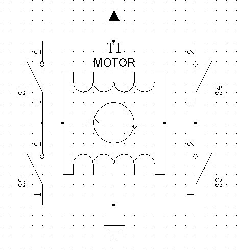
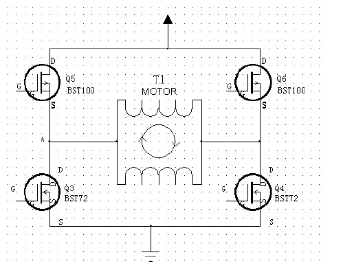
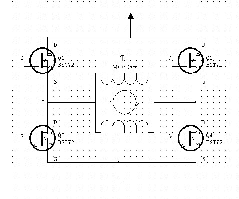
To control the positive and negative rotation of the motor, it is necessary to provide the positive and negative voltage to the motor, which requires a four-way switch to control the voltage of the two inputs of the motor. When switches S1 and S4 are closed, the current flows from the left end of the motor to the right end of the motor, and the motor rotates in one direction; When the switches S2 and S3 are closed, the current flows from the right end of the motor to the left end of the motor, and the motor rotates in the other direction. The equivalent circuit diagram of the H-bridge driving principle is shown in Figure 1.
Commonly used electronic switching devices are relays, transistors, MOS tubes, IGBT and so on. Ordinary relays are mechanical devices with limited switching times and slow switching speed. And the relay is inductive load, the interference to the circuit is relatively large. However, the relay can separate the control part from the controlled part to realize the control of the big signal by the small signal, and the relay is often used in high voltage control. The transistor is a current-driven device, the base current is IB, the collector current is IC, the amplification factor of the transistor is β, if IB*β>=IC, the transistor is in a saturated state, can be used as a switch. To make the triode in the switching state, IB= IC/β, the current of the triode driver tube is proportional to the current at the output end of the triode, if the output current of the triode is relatively large, the requirements for the triode driver end are relatively high. MOS tube is a voltage driven device. For NMOS, as long as the gate voltage is higher than the source voltage, the saturation conduction of NMOS can be achieved. The energy loss of MOS tube on and off is only the charge and discharge of the parasitic capacitance between the gate and the source, and the driving end of MOS tube is not high. At the same time, the MOS terminal can achieve a large current output, so it is generally used in places where large currents are required. IGBT is a device that combines the advantages of triode and MOS tube, and is generally used for more than 200V.
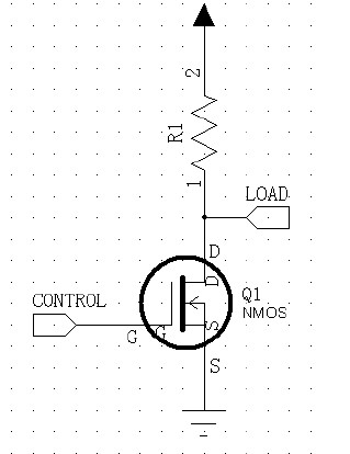
In this design, the working current of the motor is 3.8A, the working voltage is 24V, the control end of the motor drive is 51 series single-chip microcomputer, and the maximum filling current is 30mA. Therefore, MOS tube is used as the switching device of H bridge. MOS tubes are divided into NMOS and PMOS, and the manufacturing process of the two tubes is different, and the control method is different. NMOS switching requires the gate voltage to be greater than the source voltage (10V-15V), while PMOS switching requires the gate voltage to be less than the source voltage (10V-15V). In this design, 24V single power supply is used, and the on-off control of NMOS tube is shown in Figure 2. As long as the G-pole voltage is within the range of 10-15V, NMOS tube can be saturated and switched off. When the G-pole voltage is 0, NMOS tube will be turned off.
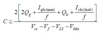
Among them: Qg = gate charge of high-end FET, f = operating frequency, ICbs (leak) = bootstrack capacitance leakage current, Iqbs (max) = maximum VBS static current, VCC = voltage source of logic circuit, Vf = forward voltage drop of bootstrack diode, VLS = low end FET or voltage drop on load, VMin = minimum voltage between VB and VS, Qls = charge required for level conversion per cycle (typically 5nC for 500V/600V MGD, and 20 nC for 1200V MGD).
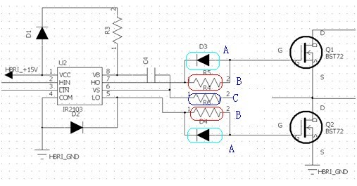
In the figure, D1 is the bootstrap diode and C4 is the bootstrap capacitor. The larger the value of the capacitor, the better. The value of the capacitor is closely related to the operating frequency of IR2103. The larger the value of the capacitor, the lower the operating frequency. The leakage current of the capacitor has a great influence on the performance of the system. The bootstrap diode has to withstand all the voltage of the system, and the forward voltage drop of the bootstrap diode also affects the selection of the bootstrap capacitor, and the switching speed of the bootstrap diode also directly affects the operating frequency of the system. The boost waveform of the bootstrap circuit obtained from the oscilloscope is shown in Figure 7 below:
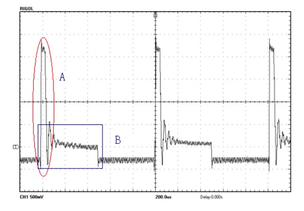
Due to the inductance generated by the lead between the driver and the MOSFET gate, the lead of the ground loop, etc., as well as the parasitic inductance inside the IC and FET, the MOSFET gate will ring when opened, which increases the switching loss of the MOSFET on the one hand, and the EMC is not well controlled. A resistor is connected in series between the gate of the MOSFET and the output of the driver IC (as shown by B in Figure 9). This resistor is called the "gate resistor ", and its role is to adjust the switching speed of the MOSFET, reduce the gate ringing phenomenon, reduce EMI, and can also play a current limiting role in the charge and discharge of the gate capacitor. The introduction of this resistance slows down the switching speed of the MOS tube, but reduces EMI and makes the gate stable.
3 Hardware Testing
In order to test the performance of the driver, 25D60-24V DC motor is selected for closed-loop control. The rated power of the motor is 60W, the rated speed is 2800rpm, the rated voltage is 24V, and the rated current is 3.8A. The maximum speed of the motor can reach 2910rpm, the minimum speed of the motor starting is 44rpm, and there is no obvious heating phenomenon when the rotation is blocked. In order to test the stability of the circuit, the motor works for more than 8 hours for three consecutive days, and the heat of the circuit is small; In order to test the impact resistance and anti-interference ability of the circuit, the system is switched between on and off continuously for many times, and there is no fault in the circuit work; In addition, the system can work normally under sudden increase of load. Therefore, it fully meets the needs of the drive, and in the design process, in order to prevent the sudden rise of the starting and braking current, the circuit has a large current redundancy, the highest current in the circuit can reach 8A, effectively ensuring the stability of the circuit, and has a strong anti-interference ability.
4 Conclusion
In this paper, a kind of high power DC motor drive circuit is designed and implemented. From the selection of devices to the realization of the system, various problems that may occur in the circuit design process are analyzed and discussed in detail, and the above problems are solved through theoretical calculation and engineering practice. The circuit has strong robustness and wide practicability, and is especially suitable for driving high-power DC motors.
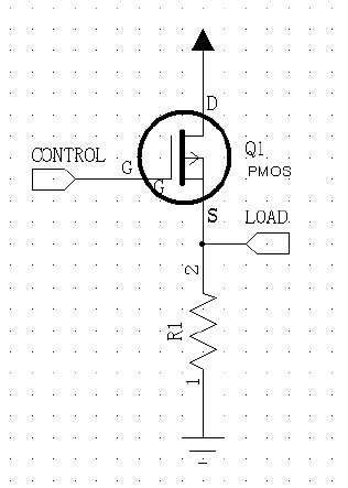
10V<VCC-Vg<15 when the PMOS is turned on. When VCC>15V, to make the PMOS conduction, the G pole voltage is VCC-15V. The on-off and off of PMOS are switched between the power supply voltage VCC and VCC-15V, and the control is inconvenient when the power supply voltage VCC is larger. Comparing FIG. 2 and FIG. 3, we can see that NMOS is located below the load, while PMOS is located above the load. By replacing the switches in FIG. 1 with NMOS and PMOS, the H-bridge composed of MOS tubes can be formed, as shown in FIG. 4.
2.3 H-bridge controller
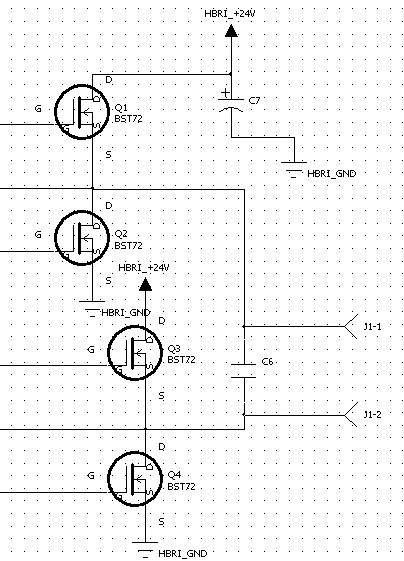
In the drive of H bridge, in addition to considering the boost circuit of the upper tube, it is also necessary to consider that the upper tube and the lower tube (Q1 and Q3 in Figure 5) with the same arm of the H bridge cannot be switched on at the same time. If the upper tube and the lower tube are on at the same time, it is equivalent to a short circuit from the power supply to the ground, which may burn the MOS tube or the power supply, even if the short circuit phenomenon for a short time will cause the MOS heat. In power control, the method of inserting a "dead zone" in two state transitions is generally used to prevent instantaneous short circuits. When selecting the H-bridge controller, it is best to meet the above two logic conditions and use a large enough drive current to drive the NMOS.
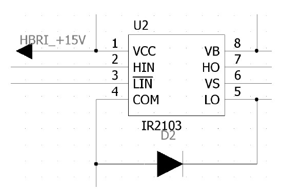
In this system, IR2103 is used as NMOS controller, IR2103 has integrated booster circuit inside, and only needs a bootstrap capacitor and a bootstrap diode outside to complete the bootstrap boost. The IR2103 has an internal dead zone riser, which can be inserted during each state transition, while ensuring that the state of the upper and lower tubes is opposite. The H-bridge half-bridge circuit composed of IR2103 and NMOS is shown in Figure 6 below:
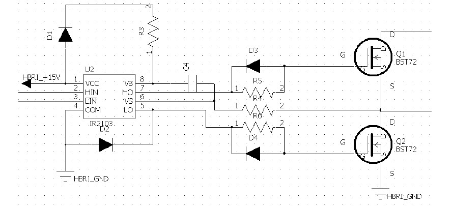
FIG. 6 H-bridge half-bridge circuit composed of IR2103 and NMOS tube
免责声明: 本文章转自其它平台,并不代表本站观点及立场。若有侵权或异议,请联系我们删除。谢谢! Disclaimer: This article is reproduced from other platforms and does not represent the views or positions of this website. If there is any infringement or objection, please contact us to delete it. thank you! |

WeChat Official Account

WeChat Service
 Email
Email QQ
QQ 13823761625
