
Analog circuit designers take great pains to make amplifiers stable when designing them. However, in the real world, there are always many situations that cause amplifiers to oscillate
Different types of loads may cause the amplifier to sing;
Poorly designed feedback networks can cause instability
Inadequate power bypasses can also cause problems
The input and output as a single-port system may also self-oscillate;
……
In order to solve these problems, today we will discuss with you the common causes of oscillation and remedies.
Basic knowledge
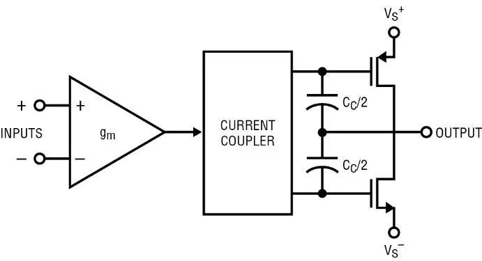
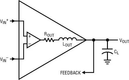
Figure 1a shows a block diagram of an off-rail to rail amplifier. The input controls the gm box, which drives the gain node and is buffered at the output. Compensation capacitor Cc is the main frequency response component. The Cc return pin should be grounded, if there is such a pin; But operational amplifiers are traditionally ungrounded, and capacitor current returns to one or both power sources. Figure 1b is a block diagram of the simplest rail-to-rail output amplifier. The output current of the input box gm is sent through a "current coupler", which splits the drive current into two parts and provides it to the output transistor. The frequency response is determined by two Cc/2s, which are actually in parallel.
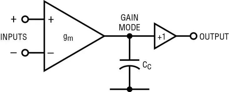
Figure 1a: Typical track-to-track operational amplifier topology
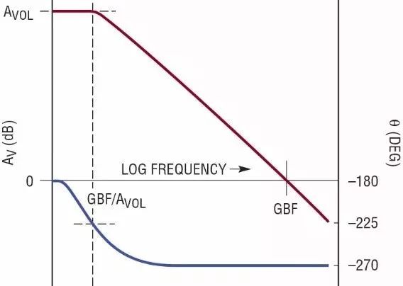
A less frequently discussed topic is gain margin, although this is an equally important parameter. When the phase margin is reduced to zero at some higher frequency, the amplifier will oscillate if the gain is at least 1V/V or 0dB. As shown in Figure 2, when the phase is reduced to 0° (or a multiple of 360°, or -180 ° as shown in the figure), the gain is about -24dB at around 1GHz. This is a very low gain, and no oscillation occurs at this frequency. In practice, one wants a gain margin of at least 4dB.
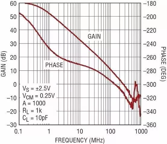
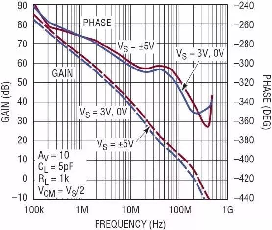
Although the LTC6268 is fairly stable under unity-gain conditions, there are a small number of deliberately unstable op amPs. By designing the amplifier compensation to be stable only at higher closed-loop gain, the design tradeoff provides higher conversion rates, wider GBF, and lower input noise than the unit-gain compensation scheme. Figure 3 shows the open-loop gain and phase of the LTC6230-10. The amplifier is intended for use with a feedback gain of 10 or greater, so the feedback net will attenuate the output by at least a factor of 10. With this feedback network, we can find the frequency at an open-loop gain of 10V/V or 20dB and find a phase margin of 58° at 50MHz (±5V power supply). At unit gain, the phase margin is only about 0° and the amplifier oscillates.
Feedback network
Speaking of oscillations, the feedback network itself can also cause oscillations. Note that in Figure 4, we put a parasitic capacitor in parallel with the feedback divider. This is inevitable, each terminal of each component on the board has about 0.5pF parasitic capacitance to the ground, and there is a parasitic capacitance of the line.
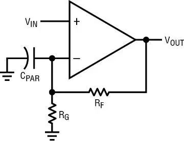
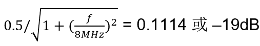
At 0° phase, 22dB of the amplifier is multiplied by -19dB of the feedback divider to produce a +3dB loop gain, and the circuit oscillates. In order to function properly in the presence of parasitic capacitance, we must reduce the value of the feedback resistor so that the feedback pole far exceeds the unit-gain frequency of the loop. The ratio of poles to GBF must be at least 6 times.
The op amp input itself may also have a considerable capacitance, as does the Cpar. In particular, low-noise and low-VOS amplifiers have large input transistors and may have larger input capacitors than other types of amplifiers, which are loaded onto the amplifier feedback network. We need to consult the data table to understand how much capacitor will be in parallel with the Cpar. Fortunately, the LT6268 has only a 0.45pF capacitance, which is very low for such a low noise amplifier. A circuit with parasitic capacitors can be simulated using ADI's free macro model running on LTspice®.
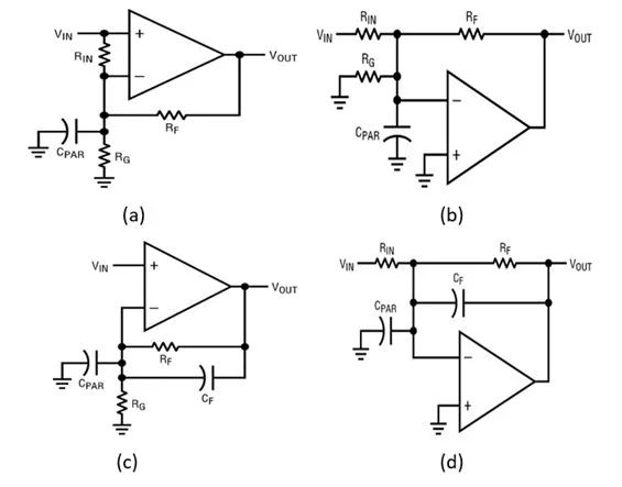
● Figure 5b shows a negative output configuration. Rg still performs loop attenuation without changing the closed-loop gain. In this case, the input impedance is free from "Rg" interference, but noise, offset, and bandwidth parameters deteriorate.
● Figure 5c shows the optimal method for compensating Cpar in the in-phase amplifier. If we set Cf* Rf = Cpar * Rg, we have a "compensated attenuator" so that the feedback divider now has the same attenuation at all frequencies and solves the Cpar problem. Mismatches in the product will cause "bumps" in the amplifier's passband and "shelf" in the response curve (where the low-frequency response is flat but changes to another flat line segment near f = 1/2 * Cpar * Rg). Figure 5d shows the equivalent Cpar compensation for a negative output amplifier. The frequency response must be analyzed to find a correct Cf, and the bandwidth of the amplifier is part of that analysis.
Here are some reviews of current feedback amplifiers (CFA) in turn. If the amplifier in Figure 5a is a CFA, then "Rin" does little to change the frequency response because the negative input is a very low impedance and actively copies the positive input. The noise indicator will be slightly degraded, and the additional negative input bias current will actually be in the form of Vos/Rin. Again, the circuit in Figure 5b is not altered by "Rg" in terms of frequency response. The inverting input is not just a virtual ground, it is a real ground low impedance and has allowed Cpar (negative output mode only!). . The DC error is similar to the situation shown in Figure 5a. Figure 5c and 5d May be the preferred solution for voltage input opamps, but CFA does not allow a direct feedback capacitor without oscillation at all.
Load problem
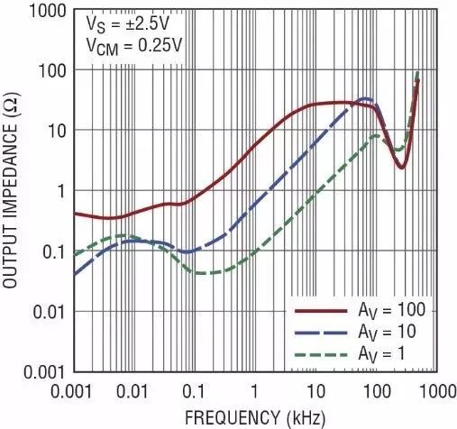
Just as feedback capacitors can harm the phase margin, so can load capacitors. Figure 6 shows how the LTC6268 output impedance varies with frequency at several gain setpoints. Note that the unit-gain output impedance is lower than the output impedance at higher gain. Full feedback enables the open-loop gain to reduce the inherent output impedance of the amplifier. Therefore, in Figure 6, the output impedance at a gain of 10 is generally 10 times that of the output impedance at unit gain. Since the feedback attenuator reduces the loop gain, the loop gain is 1/10, otherwise it would reduce the closed-loop output impedance. The open-loop output impedance is about 30, which is evident in the high frequency flat region of the curve with a gain of 100. In this region, from the gain bandwidth frequency /100 or so to the gain bandwidth frequency, there is not enough loop gain to reduce the open-loop output impedance.
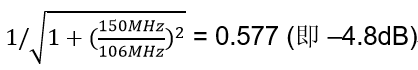
–atan(150MHz/106MHz) = –55°
And a gain
Multiplying the gain cyclically, we get 360° phase and +0.2dB gain, again an oscillator. 50pF appears to be the minimum load capacitance that will force the LTC6268 to oscillate.
The most common way to prevent the load capacitor from causing oscillations is to simply give the capacitor a small resistance value in series after the feedback connection. Resistance values of 10Ω to 50Ω will limit the phase lag that can be caused by capacitive loads and isolate the amplifier from low capacitive impedances at very high speeds. Disadvantages include DC and low-frequency errors that vary with the load resistance characteristics, limits on the capacitive load frequency response, and signal distortion if the load capacitance is not constant as the voltage changes.
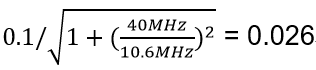
Increasing the closed-loop gain of the amplifier often prevents oscillations caused by the load capacitance. Running the amplifier at a higher closed-loop gain means that at frequencies where the loop phase is ±360°, the feedback attenuator also attenuates the loop gain. For example, if we use the LTC6268 with a closed-loop gain of +10, then we see that the amplifier has a gain of 10V/V or 20dB at 40MHz with a phase lag of 285°. To excite the oscillation, an output pole is required, resulting in an additional 75° lag. By -75 ° = -ATAN (40MHz/Fpole) → Fpole = 10.6MHz, we can find the output pole. This pole frequency is derived from a 500pF load capacitor and an output impedance of size 30. The output pole gain is
Since the unloaded open-loop gain is 10, we get that the loop-wound gain at the oscillation frequency is 0.26, so this time we do not produce an oscillation, at least not one caused by a simple output pole. Thus, by increasing the closed-loop gain, we increase the load capacitance tolerance from 50pF to 500pF.
In addition, unterminated transmission lines are also very bad loads because they introduce "runaway" impedance and phase changes that repeat with frequency (see the impedance of an unterminated 9-foot cable in Figure 7).
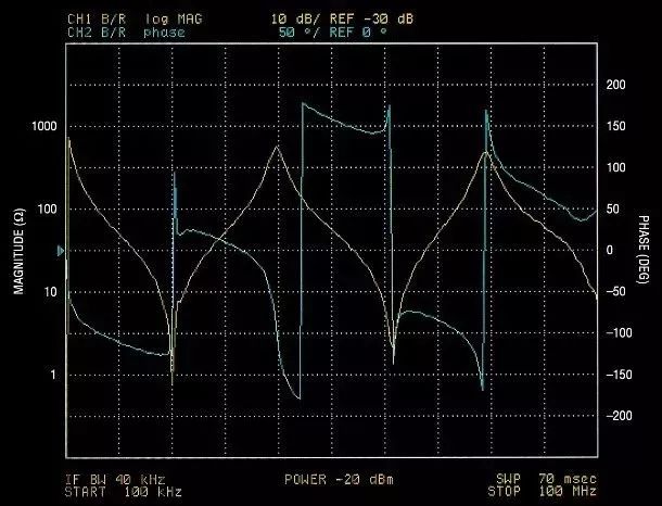
Figure 8 shows a more complete output impedance model. The ROUT term is the same as we discussed in LTC6268, which is also 30Ω, and here we add another Lout term. This is a combination of physical inductance and electronic equivalent inductance. The physical package, bonding wire, and external inductance add up to 5nH to 15nH, and the smaller the package, the smaller the number.
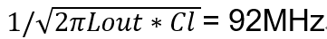
Located just inside the LTC6268 passband. In fact, this series resonant circuit is loaded onto the output during resonance, seriously altering the phase of the loop near the resonant frequency. Unfortunately, Lout is not mentioned in the amplifier's data sheet, but its effect can sometimes be seen on the open-loop output impedance diagram. In short, this effect is not important for amplifiers with bandwidths less than 50MHz or so.
One solution is shown in Figure 9. Rsnub and Csnub form what is called a "shock absorber", whose purpose is to reduce the Q value of the resonant circuit so that the resonant circuit does not add a very low resonant impedance to the amplifier output. The value of Rsnub is usually estimated as the reactance of CL at resonance (in this case -j35Ω) to reduce the Q value of the output resonant circuit to about 1. Resize Csnub so that Rsnub is fully inserted at the output resonant frequency, i.e., Csnub's reactance <.
Strange impedance
Many amplifiers have a slightly abnormal input impedance at high frequencies. This is most true of amplifiers with two input transistors in series, such as the Darlington configuration. Many amplifiers have npn/pnp transistor pairs at the input, which behave with frequency similar to the Darlington configuration. The real part of the input impedance becomes negative at some frequencies (generally much higher than GBF). The inductive source impedance will resonate with the input and board capacitors, and a negative real component may cause oscillations. When driven with an unterminated cable, this can also cause oscillations at many repeat frequencies. If the input inevitably uses a long inductive wire, then several resistors in series that can absorb energy can be used to disconnect the wire, or a medium impedance shock absorber (about 300Ω) can be installed on the amplifier input lead.
Power source
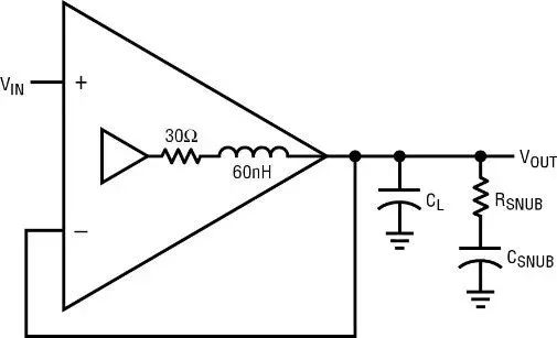
The final source of oscillation to consider is the power bypass. Figure 10 shows a portion of the output circuit. LVS+ and LVS - are unavoidable series inductors for packaging, IC bonding wires, the physical length of the bypass capacitor (which is inductive like any conductor), and circuit board wiring. Also included are external inductors that connect the local bypass component to the rest of the power bus (if not the power plane). Although 3nH to 10nH May not seem like much, at 200MHz, it is 3.8 to j12Ω. If the output transistor conducts a large high-frequency output current, there will be a voltage drop at both ends of the supply inductor.
Conclusion
In summary, designers need to consider the parasitic capacitance and inductance associated with each op amp terminal, as well as the nature of the load. Amplifiers are designed to be stable in nominal environments, but each application requires its own analysis.
免责声明: 本文章转自其它平台,并不代表本站观点及立场。若有侵权或异议,请联系我们删除。谢谢! Disclaimer: This article is reproduced from other platforms and does not represent the views or positions of this website. If there is any infringement or objection, please contact us to delete it. thank you! |

WeChat Official Account

WeChat Service
 Email
Email QQ
QQ 13823761625
