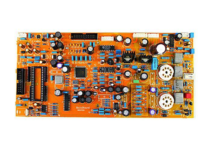
Reasonable layout of PCB components in chip processing is the basic premise of designing high-quality PCB drawings. The requirements of component layout mainly include installation, force, heat, signal and aesthetic requirements.

1. Installation
It refers to a series of basic requirements put forward in order to smoothly install the circuit board into the chassis, shell, and slot in a specific application, without space interference, short circuit and other accidents, and make the specified connector in the designated position on the chassis or shell.
2. Force
In the chip processing, the circuit board should be able to withstand various external forces and vibrations during installation and work. Therefore, the circuit board should have a reasonable shape, and the positions of various holes (screw holes, special-shaped holes) on the board should be reasonably arranged. Generally, the distance between the hole and the edge of the plate should be at least greater than the diameter of the hole. At the same time, it should also be noted that the weakest section of the plate caused by the special-shaped hole should also have sufficient bending strength. In particular, the connectors that directly "extend" out of the equipment housing on the board should be reasonably fixed to ensure long-term reliability.
3. Get hot
For high-power, serious heating devices, in addition to ensuring heat dissipation conditions, but also pay attention to placing in the appropriate position. Especially in sophisticated analog systems, special attention should be paid to the adverse effects of the temperature field generated by these devices on the fragile pre-amplifier circuit. Generally, the part with very large power should be made into a module separately, and certain thermal isolation measures should be taken between the signal processing circuit.
4. Signals
Signal interference is the most important factor to consider in PCB layout design. The most basic aspects are: the weak signal circuit and the strong signal circuit are separated or even isolated; The AC part is separated from the DC part; The high frequency part is separated from the low frequency part; Note the direction of the signal line; Layout of ground wire; Appropriate shielding, filtering and other measures.
5. Beautiful
We should not only consider the orderly placement of components, but also consider the beautiful flow of the line. Because the general layman sometimes more emphasis on the former, in order to one-sided evaluation of the advantages and disadvantages of circuit design, in order to the image of the product, the former should be given priority when the performance requirements are not harsh. However, in high-performance occasions, if you have to use dual panels, and the circuit board is also packaged inside, usually can not see, you should prioritize the beauty of the line.
免责声明: 本文章转自其它平台,并不代表本站观点及立场。若有侵权或异议,请联系我们删除。谢谢! Disclaimer: This article is reproduced from other platforms and does not represent the views or positions of this website. If there is any infringement or objection, please contact us to delete it. thank you! |


