
Today, the design of high-speed electronic systems is difficult to succeed without a thorough understanding of the chip, package structure, and power supply system characteristics of the PCB. In fact, in order to meet the lower power supply voltage, faster signal turnover speed, higher integration and many increasingly challenging requirements, many companies at the forefront of electronic design in the product design process in order to ensure the integrity of the power supply and signal, the analysis of the power supply system invested a lot of money, manpower and material resources.
The analysis and design of power supply systems (PDS) is becoming increasingly important in the field of high-speed circuit design, especially in the computer, semiconductor, communications, networking and consumer electronics industries. With the inevitable further scaling down of VLSI technology, the supply voltage of integrated circuits will continue to decrease. As more and more manufacturers move from 130nm technology to 90nm technology, it is expected that the supply voltage will drop to 1.2V or even lower, while the current will also increase significantly. From the perspective of DC IR voltage to AC dynamic voltage fluctuation control, because the allowable noise range is getting smaller and smaller, this development trend brings great challenges to the design of power supply system.
PCB power supply system design overview
Usually in AC analysis, the input impedance between power sources is an important observation used to measure the characteristics of the power supply system. The determination of this observation is evolved into the calculation of IR pressure drop in DC analysis. Whether in the DC or AC analysis, the factors that affect the characteristics of the power supply system are: the layering of the PCB, the shape of the power board layer plane, the layout of the components, the distribution of holes and pins, and so on.
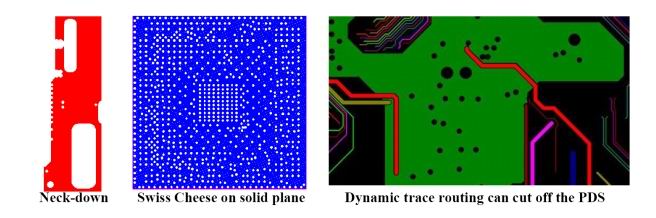
Figure 1: Some common physical structural designs on PCBS that increase current path resistance.
The concept of input impedance between power sources can be applied to the simulation and analysis of the above factors. For example, a very broad application of the input impedance of a power supply is to evaluate the placement of decoupled capacitors on a board. With a certain number of decoupling capacitors placed on the board, the unique resonance of the board itself can be suppressed, thereby reducing the generation of noise, and also reducing the edge radiation of the board to alleviate electromagnetic compatibility problems. In order to improve the reliability of the power supply system and reduce the manufacturing cost of the system, the system design engineer must often consider how to cost-effectively select the system layout of decoupling capacitors.The power supply system in the high-speed circuit system can usually be divided into three physical subsystems: chip, integrated circuit package structure and PCB. The power grid on the chip is composed of several layers of metal layers placed alternately, each layer of metal is composed of metal strips in the X or Y direction to form the power supply or ground grid, and the different layers of metal strips are connected through the hole.
For some high-performance chips, both the core and the power supply of IO are integrated with many decoupling units. The integrated circuit package structure, like a reduced PCB, has several layers of a complex shape of the power supply or floor plate. On the upper surface of the package structure, there is usually a position for mounting the decoupling capacitor. PCB usually contains a continuous area of large power supply and floor plate, as well as some large and small discrete decoupling capacitor components, and power rectifier module (VRM). The Bonding line, C4 bump, and solder ball connect the chip, package, and PCB together.
The entire power supply system should ensure that each integrated circuit device is provided with a stable voltage within the normal range. However, switching currents and parasitic high-frequency effects in those power-supply systems always introduce voltage noise. The voltage variation can be calculated by the following formula:

Here ΔV is the voltage fluctuation observed at the device, and ΔI is the switching current. Z is the input impedance observed at the device between the power supply and the ground of the entire power supply system. In order to reduce voltage fluctuations, the resistance between the power supply and the ground should be kept low. In the DC case, since Z becomes a pure resistance, the low resistance corresponds to a low power supply IR voltage drop. In the case of AC, the low resistance can also reduce the transient noise generated by the switching current. This, of course, requires Z to remain small over a wide frequency band.
Note that power supply and ground are often used as signal loops and reference planes, so there is a close relationship between the power supply system and the signal distribution system. However, due to space constraints, the noise phenomena and current loop control problems of power supply systems introduced by synchronous switching noise (IO SSO) will not be discussed here. The following sections will ignore the signal system and focus solely on the analysis of the power supply system.
Dc IR voltage drop
Due to the small characteristic size of the chip's Power Grid (a few microns or even smaller), the resistance loss in the chip is serious, so the IR voltage drop in the chip has been extensively studied. In the following cases, the IR pressure drop on the PCB (in the range of tens to hundreds of millivolts) will also have a greater impact on high-speed system design.
Swiss-Chess structure, Neck-Down structure and dynamic wiring caused the board plane to be divided on the power supply board layer (FIG. 1). The number of device pins, holes, welding balls and C4 convex points that current passes through on the power supply plate layer is not enough, the thickness of the power supply plate is insufficient, and the current path is unbalanced. The system design requires low voltage, high current, and a tight voltage floating range.
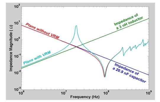
Figure 3: Input impedance of a flat plate with and without a power rectifier module.
For example, a high-density and high-pin device with a large number of holes and backpads often forms a so-called Swiss-Chess structure effect on the chip package structure and the power distribution layer of the PCB. The Swiss-Chess structure produces many tiny metallic regions with high resistivity. According to the power supply system has such a high resistance current path, the voltage or current sent to the PCB components may be lower than the design requirements. Therefore, a good DC IR voltage drop simulation is the key to estimate the allowable voltage drop range of the power supply system. Through the analysis of various possibilities, the design scheme or rules are provided for the layout and wiring.
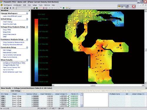
Wiring engineers, systems engineers, signal integrity engineers, and power design engineers can also incorporate IR voltage drop analysis into the constraint manager as a final validation tool (DRC) for design rule verification of each power and grid meter on the PCB. This design process analyzed by automated software can avoid layout problems in complex power supply system structures that cannot be detected by visual inspection or even experience. Figure 2 shows that IR voltage drop analysis can accurately pinpoint the distribution of critical voltage and current in a power supply system on a high performance PCB.
Impedance analysis of AC source
Many people know that a pair of metal plates constitute a flat capacitor, so they think that the characteristics of the power supply plate layer is to provide a flat capacitor to ensure the stability of the supply voltage. At lower frequencies, when the signal wavelength is much larger than the plate size, the power board and floor do constitute a capacitor.
However, when the frequency increases, the characteristics of the power supply layer begin to become complicated. More specifically, a pair of plates form a plate transmission line system. The noise between the power supply and the ground, or the corresponding electromagnetic field, is propagated between the boards according to the transmission line principle. When the noise signal travels to the edge of the plate, a portion of the high-frequency energy will radiate out, but a larger portion of the energy will be reflected back. Multiple reflections from different boundaries of the plate constitute the resonance phenomenon in the PCB.
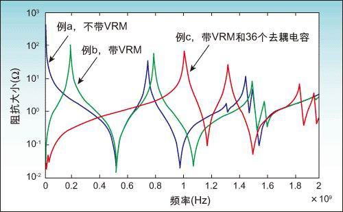
Figure 4: PCB input impedance curves calculated by PowerSI in three Settings. (a) Does not include a power supply rectifier module; (b) Includes a power supply rectifier module; (c) Includes a power supply rectifier module and some decoupling capacitors.
In AC analysis, the power source ground impedance resonance of PCB is a unique phenomenon. Figure 3 shows the input impedance of a pair of power supply layers. For comparison, the impedance characteristics of a pure capacitor and a pure inductor are also drawn. The size of the board is 30cm×20cm, the spacing between the boards is 100um, and the filling medium is FR4 material. The power supply rectifier module on the board is replaced by a 3nH inductor. The pure capacitance impedance characteristic is shown by a 20nF capacitor. As can be seen from the figure, when there is no power rectifier module on the board, the impedance characteristics of the plate (red line) and the capacitance (blue line) are the same in the frequency range of tens of megabits. Above 100MHz, the impedance characteristics of the plate are inductive (along the green line). After the frequency range of several hundred megabits, the appearance of several resonant peaks shows the resonant characteristics of the plate, and the plate is no longer purely inductive.
At this point, it is clear that a low-resistance power supply system (from DC to AC) is the key to obtaining low voltage fluctuations: reducing the inductance action, increasing the capacitance action, and eliminating or reducing those resonant peaks are the design goals.
In order to reduce the impedance of the power supply system, the following design guidelines should be followed:
1. Reduce the distance between the power supply and the floor layer;
2. Increase the size of the plate;
3. Increase the dielectric constant of the filling medium;
4. Use multiple power supplies and floor layers.
However, due to manufacturing or some other design considerations, design engineers also need to use some more flexible and effective methods to change the impedance of the power supply system. In order to reduce the impedance and eliminate those resonant peaks, placing discrete decoupling capacitors on the PCB has become a common method.
Figure 4 shows the input impedance of a power supply system calculated using Sigrity PowerSI at three different Settings:
a. No power supply rectifier module, no decoupling capacitor placed on the board.
b. The power rectifier module is simulated with a short circuit, and no decoupling capacitor is placed on the board.
c. The power rectifier module is simulated by a short circuit, and the decoupling capacitor is placed on the board.
As can be seen from the figure, example a blue line, the input impedance of the power supply system observed at the location of the integrated circuit chip is capacitive at low frequencies. As the frequency increases, the first natural resonance peak appears at the 800MHz frequency. The wavelength of this frequency corresponds to the size of the power supply floor plate.
In the green line of example b, the input impedance is inductive at low frequencies. This corresponds exactly to the loop inductance from the position of the integrated circuit chip to the power rectifier module. This loop inductor and plate capacitor together introduce a resonant peak at 200MHz.
In the red line of example c, after some decoupling capacitors are placed on the board, the 200MHz resonant peak is moved to a very low frequency (<20MHz), and the peak of the resonant peak is also reduced a lot. The first strong resonant peak appears at about 1GHz. It can be seen that by placing discrete decoupling capacitors on the PCB, the power supply system can achieve a low and smooth AC impedance response over the main operating frequency range. Therefore, the noise of the power supply system will also be low.
The placement of discrete decoupling capacitors on the board allows the designer to flexibly adjust the impedance of the power supply system to achieve lower power ground noise. However, how to choose the placement, how many and what kind of decoupling capacitors are still a series of design problems. Therefore, it is often necessary to seek the best decoupling solution for a particular design, use the appropriate design software and carry out a large number of power supply system simulations.
Collaborative design concept
Figure 4 actually reveals another very important fact, namely that discrete decoupling capacitors placed on the PCB can only reach the frequency range of a few hundred megahertz. At higher frequencies, the parasitic inductance of each discrete decoupling capacitor and the loop inductance (capacitor to chip) of the board and through the hole will greatly reduce the decoupling effect, and the input impedance of the power supply system cannot be further reduced simply by placing discrete decoupling capacitors on the PCB. From a few hundred megahertz to higher frequency ranges, the interboard capacitors of the power supply system in the package structure, as well as discrete decoupling capacitors placed on the package structure, will come into play. In the GHz frequency range, in-chip capacitors between power grids and in-chip decoupling capacitors are the only decoupling solutions.
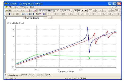
Figure 5 shows an example where the red line is the input impedance obtained by placing some discrete decoupling capacitors on a PCB. The first resonant peak appears at 600MHz to 700MHz. After considering the package structure, the inductance of the additional package structure moves the resonance peak to about 450MHz, see the blue line. After the chip power supply system is included, the decoupling capacitor in the chip removes those high-frequency resonant peaks, but at the same time introduces a very weak 30MHz resonant peak, see green line. This 30MHz resonance is represented in the time domain as a voltage trough in the IF envelope of the high-frequency flip signal.
In-chip decoupling is very effective, but the cost is to use up valuable space in the chip and consume more leakage current. Moving the decoupling capacitor in the chip to the package structure may be a good compromise, but requires the designer to have knowledge of the entire system from the chip and package structure to the PCB. But in general, PCB designers do not have access to the design data of the chip and package structure and the corresponding simulation software packages. For integrated circuit designers, they usually do not care about the lower end of the package and board design. However, it is obvious that using the concept of collaborative design to optimize the analysis and design of the whole system, chip-package-circuit board power supply system is the future development trend. Some companies at the forefront of electronic design actually already do this.
免责声明: 本文章转自其它平台,并不代表本站观点及立场。若有侵权或异议,请联系我们删除。谢谢! Disclaimer: This article is reproduced from other platforms and does not represent the views or positions of this website. If there is any infringement or objection, please contact us to delete it. thank you! |

WeChat Official Account

WeChat Service
 Email
Email QQ
QQ 13823761625
