
Class D audio amplifier has the advantages of high efficiency, energy saving and miniaturization, and is widely used in many fields such as portable products, home AV equipment and car audio. The Class D audio power amplifier designed in this paper is mainly based on the following three considerations: ensuring high fidelity, improving efficiency and reducing volume. This paper designs a Class D audio power amplifier which works at 5V supply voltage and adopts PWM. The whole system includes input amplifier stage, error amplifier, comparator, internal oscillation circuit, drive circuit, full bridge switching circuit and reference circuit. By introducing feedback technology to reduce the THD index of the system, the dual-channel inverse width modulation scheme not only reduces the static power consumption of the Class D audio power amplifier, but also removes the low-pass filter at the output end of the Class D audio power amplifier and reduces the volume of the system.
1 Class D audio amplifier system design
The system structure of the Class D audio power amplifier designed in this paper is shown in Figure 1. The structure of the amplifier is based on the two-sided natural sampling technology, and the information contained in the output at any time is twice that of the single-sided sampling scheme. Through the two-sided natural sampling, a large number of distortion components in the output audio signal can be removed outside the audio bandwidth range that can be sensed by the human ear. The purpose of removing the low-pass filter at the output end of Class D audio power amplifier is achieved.
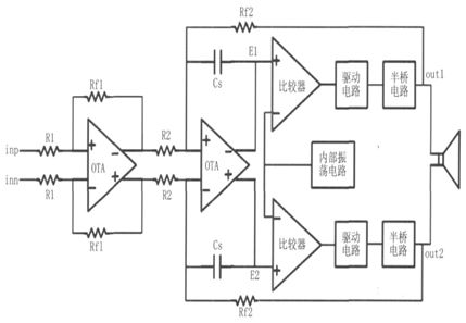
In Figure 1, the currents I1 and I2 that charge and discharge the capacitor Cs are jointly determined by Vout1, Vout2, Vin, R1, Rf1, R2, and Rf2, where the resistance and capacitor must have good linearity and matching to obtain good closed-loop performance.
The model of an open-loop Class D audio power amplifier is shown in Figure 2.
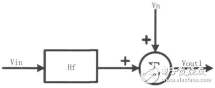
The system output is:

The total harmonic distortion of an open-loop system is:
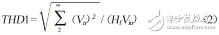
In formula (2), Vin is the input signal of the amplifier, Vn is the introduced harmonic distortion, and Hf is the transfer function数。
The model of a Class D audio power amplifier with a feedback loop is shown in Figure 3.
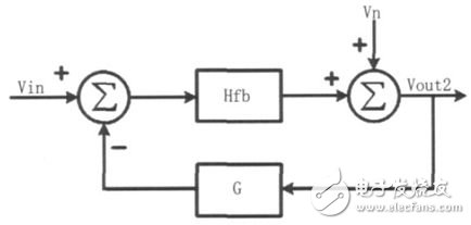
The output of the system is:
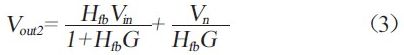
Where Hfb is the transfer function of the closed-loop model and G is the feedback gain. In order to obtain the same magnification, the transfer function is designed as:

Then formula (3) becomes:

The total harmonic distortion of the closed system is:
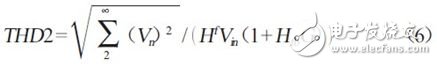
By comparing equations (2) and (6), it can be seen that the THD of the closed-loop system with feedback loop is 1/ (1+HfbG) of the THD of the open-loop system, that is, the THD of the system is reduced by the feedback structure.
2 unit circuit design and implementation
The system unit circuit mainly includes: input amplifier stage, error amplifier, comparator, drive circuit, full bridge switch circuit, internal oscillation circuit and reference circuit.
2.1 Input amplifier stage
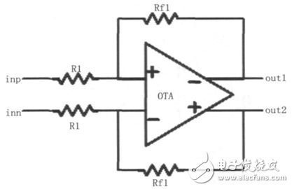
The input amplifier stage of the Class D audio power amplifier is based on the closed-loop structure of the operational amplifier (OTA), and its structure is shown in Figure 4. It is used to adjust the input audio signal level and amplify the signal according to the needs, so that the input signal can meet the requirements of the post-stage circuit in terms of amplitude. The gain of the input amplifier stage can be determined by setting the resistance values of Rf1 and R1.
2.2 Comparator
The comparator circuit used in this paper is shown in Figure 5. The comparator circuit consists of three stages, namely, input pre-amplification stage, judgment stage (or positive feedback stage) and output digital shaping buffer stage. The pre-amplifier stage is realized by an active loaded differential amplifier, whose amplification ratio is not very large, which is used to amplify the input signal to improve the sensitivity of the comparator, and to isolate the input signal of the comparator from the switching noise from the positive feedback stage. The judgment stage is used to further amplify the signal of the pre-amplified stage. As the core part of the comparator, the positive feedback is achieved by cross-interconnecting the gate of m8 and m9 in the circuit, so as to have the ability to distinguish very small signals and improve the gain of this stage circuit; The output buffer stage is a self-biased differential amplifier whose input is a pair of differential signals, which is used to convert the output signal of the judgment stage into a logic level (0V or 5V), that is, the output high level VOH=VDD and the output low level VOL=GND.
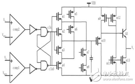
2.3 Internal oscillation circuit
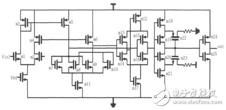
The triangular wave generation circuit structure adopted in this paper is shown in Figure 6, where m5, m6, m7 and m8 constitute two groups of constant current sources, and m9~m13 and Q1 constitute the output stage. In the circuit, the output signal VT is fed back to comparators comp1 and comp2, respectively, with reference levels VREF1 and VREF2 (VREF2)
2.4 Full bridge switch circuit
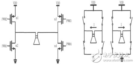
The output stage is realized by a full-bridge switching circuit composed of N and P type power switch pairs. Its structure and load current flow direction are shown in Figure 7.
2.5 Drive Circuit
The structure of the drive circuit is shown in Figure 8. The circuit can effectively adjust the dead time (N-type and P-type power switch tubes are turned off at the same time), prevent single-arm "shoot-through" phenomenon, and protect the turn-off function. The input signal is the PWM pulse signal output by the comparator, PWM1 is used to drive the N-type power switch tube, and PWM2 is used to drive the P-type power switch tube. In order to avoid the single-arm "shoot-through" phenomenon in the full-bridge switching circuit, when the PWM signal changes from low level to high level, PWM2 should first change to high level, turn off the PMOS power switch tube, and then PWM1 should change to high level again, and turn on the NMOS power switch tube, as shown in Figure 9. On the other hand, when the PWM signal changes from high to low, PWM1 becomes low first, and the NMOS switching power tube is turned off, and then PWM2 becomes low again, and the PMOS switching power tube is turned on. In the actual circuit, the dead-time can be adjusted according to the need by controlling the control bit Tc of the delay unit. In order to reduce the distortion, the dead time must be reduced. The drive circuit uses the way of increasing the drive capacity step by step to drive the power tube, thus reducing the necessary dead time and ensuring the low distortion degree.
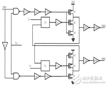
Figure 8 Drive circuit structure
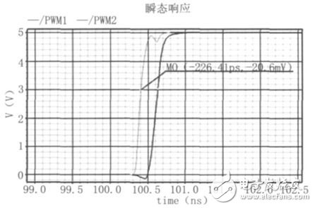
Figure 9 Dead zone time
EN is the enable signal of the control module, which normally works at a high level; When there is overcurrent, overtemperature, etc., it becomes low, and the full bridge power switching circuit is turned off.
2.6 Reference Circuit
The structure of the band-gap voltage reference source designed in this paper is shown in Figure 10, which mainly consists of two parts: the core circuit and the starting circuit.
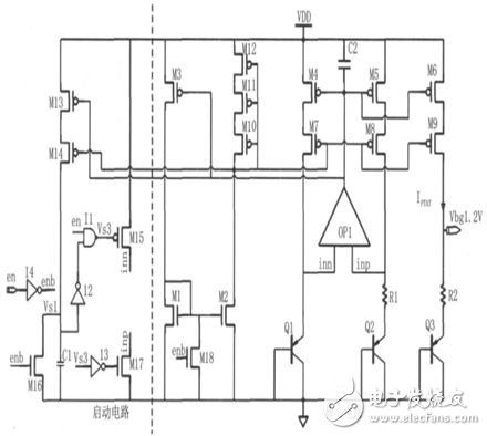
When the circuit is powered on, the bias circuit may have zero current, and it is necessary to start the circuit to ensure that the circuit can work normally. When the circuit does not work, EN, Vs1 is 0, Vs2, Vs3 is 1, M15, M17 is blocked, the op amp output is high, M3~M6 is also blocked, and the entire circuit does not consume current. When EN changes from 0 to 1, due to the action of C1, Vs1 remains 0, Vs2 is 1, and Vs3 becomes 0. At this time, M15 and M17 are switched on, inp and inn are pulled to 0 and 1 respectively, the op amp output becomes 0, M3~M6 is switched on, M13 and M14 branches begin to have current, and C1 is charged. When Vs1 exceeds the I2 threshold voltage, Vs2 becomes 0, Vs3 becomes 1, and M15 and M17 are turned off. Finally, the circuit deviates from the zero current state and starts to work normally, and the Vs1 is charged to the power supply voltage, and the entire starting circuit no longer consumes current.
3 Conclusion
In this paper, the working principle of Class D audio power amplifier based on PWM modulation technology is studied, and the THD of Class D audio power amplifier is reduced by introducing feedback technology. The necessary dead time is reduced by increasing the driving capacity step by step to ensure a lower distortion degree. By adopting the dual-channel inverse width modulation scheme, the static power consumption of the system is suppressed on the one hand, and the LC low-pass filter of the output stage is removed on the other hand, so the cost and volume of the system are reduced.
免责声明: 本文章转自其它平台,并不代表本站观点及立场。若有侵权或异议,请联系我们删除。谢谢! Disclaimer: This article is reproduced from other platforms and does not represent the views or positions of this website. If there is any infringement or objection, please contact us to delete it. thank you! |

WeChat Official Account

WeChat Service
 Email
Email QQ
QQ 13823761625
