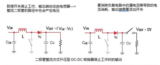
· When the diode rectifier booster DC-DC converter is turned off, the output will not change to 0V, but will output VIN-VF voltage.
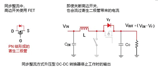
· When the synchronous rectifier booster type DC-DC converter is turned off, it will also output VIN-VF voltage due to the influence of the parasitic diode of the FET used in the high-side switch.
· Because the output voltage is very low when the load circuit is turned off, the load circuit may misoperate aa, and the current flowing through the load circuit and the voltage setting resistance will cause the standby power consumption to increase.
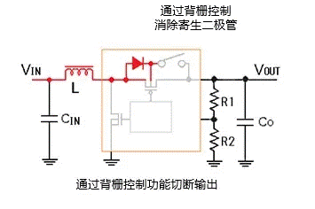
· Synchronous rectifier boost DC-DC converters with backgate control can reduce the output to 0V at shutdown by removing the parasitic diode, thereby preventing load circuit misaction and increased standby power consumption.
In this paper, we will be divided into "diode rectifier boost type DC-DC converter", "synchronous rectifier boost type DC-DC converter", "standby current consumption caused by current flowing through the voltage setting resistor" and "synchronous rectifier with back grid control function" several parts, to introduce the impact of the boost power supply on the output voltage and countermeasures.
Diode rectifier boost type DC-DC converter
In the diode rectifier mode, because there is a path from the VIN through the inductor and the rectifier diode, the VOUT will output the voltage (VIN-VF) even if the switching operation is stopped due to a shutdown. Because the voltage is still applied to the load circuit, under certain VIN voltage conditions, the load circuit will consume current, and the standby consumption current will increase. In addition, applying a half-assed low voltage to the load circuit may result in misoperation, and in some cases an output cutoff circuit is required.

Synchronous rectifier boost type DC-DC converter
In the case of synchronous rectification, the high-side switch uses the FET, and when turned OFF, the high-side switch will be off because there is no gate drive. However, the FET's parasitic diodes form a current path, so VOUT still outputs (VIN-VF) voltage.

The consumption of standby current caused by the current flowing through the voltage setting resistor
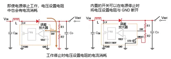
The power supply has a resistor divider connected to the VOUT to set the output voltage. At work, a current of VOUT÷ (R1+R2) will flow through this resistor. When the power supply is turned off, the VOUT voltage drops and the current flowing through the voltage setting resistor decreases, but the standby consumption current increases. This current can be reduced by increasing the resistance value, but the resistor needs to be able to carry more than 100 times the error amplifier input bias current. If it cannot carry such a large current, the output voltage VOUT will change greatly due to the input bias current fluctuation caused by temperature and other factors, thus affecting the output voltage error, so the resistance value cannot be arbitrarily increased. Pre-2000 power supply ics, many of which were bipolar products, had input bias currents of tens of microamps (μA), so a current of several milliamps (mA) was required to flow from the voltage setting resistor. However, after 2000, power ics, CMOS products have been popularized, the input bias current has been reduced to the nanoampere (nA) level, and the current flowing through the voltage setting resistor has also been reduced to the tens of microampere (μA) level. Even so, if it is a battery-powered application such as a mobile device, the current consumption of microampere (μA) level can affect the battery life and even cause problems.

In order to eliminate the current consumption caused by the voltage setting resistor and reduce the standby current consumption, some power supply products have a built-in switch that disconnects the voltage setting resistor from GND when it is turned off.
Synchronous rectification with back grid control function
A synchronous rectifier power supply IC with a high side switch FET is built into the IC, and some products have a circuit that applies bias to the back gate of the FET, and the parasitic diode can be eliminated by controlling the circuit. This switch cuts off the current path created by the FET's parasitic diode, so that the output voltage changes to 0V when it is turned off, which prevents misoperation of the load circuit and ensures a reset of the power supply. It also eliminates the current consumption caused by the voltage setting resistance and the load circuit (bringing the consumption current to zero).

免责声明: 本文章转自其它平台,并不代表本站观点及立场。若有侵权或异议,请联系我们删除。谢谢! Disclaimer: This article is reproduced from other platforms and does not represent the views or positions of this website. If there is any infringement or objection, please contact us to delete it. thank you! |


