How to achieve a cost-effective 2X10W boost dual channel solution with two LTK53107s
Date:October 22, 2024 Views:837
如何用两个LTK53107实现高性价比 2X10W升压双声道方案
---- Audio power amplifier
LPA001 – October 2023
Through the combination of two small size, high power built-in boost mono LTK53107, using one of the boost to directly supply power to the other, while saving a set of peripheral boost supporting circuits, you can achieve dual channel built-in boost 2X10W power, thereby providing cost-effective stereo solutions.
Project introduction
The LTK53107 is a mono, high-power, AB/D switchable audio power amplifier with adaptive boost. At 3.7V, the 3Ω load can reach 15W, and the 2Ω load can reach 19W, and the strong boost current ability can meet the power of its own amplifier while providing the possibility of direct power supply for another amplifier.
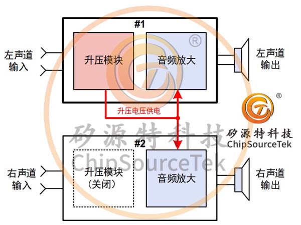
The LTK53107 chip integrates a booster module and an audio amplifier circuit. In this scheme, two LTK53107 are used. As shown in Fig.1, the booster system of #1 directly supplies power to another LTK53107 (#2) in addition to supplying power to its own amplifier. At the same time, the boost module of #2 is in a closed state (no peripheral supporting boost devices), so that only a set of peripheral inductors and Schottky diodes are needed to achieve a high-power dual-channel boost output scheme.
Provides the possibility.

Scheme advantage
➢ LTK53107 adopts ESOP-10 small volume package, two LTK53107 occupy a smaller PCB area.
➢ Two LTK53107 only requires a set of peripheral boost inductors and Schottky diodes, optimizing the peripheral components of the overall solution.
➢ LTK53107 has AB/D class switchable function, which can solve the problem of the lack of AB class in the market with high power (2X10W) dual channel built-in boost.
➢ LTK53107 has a strong boost current capability, providing instant 8A input current, can meet the dual channel power requirements.
➢ About the separate channel, with better stereo channel crosstalk suppression performance, excellent power distortion can better meet customer requirements for stereo sound quality.
Application circuit
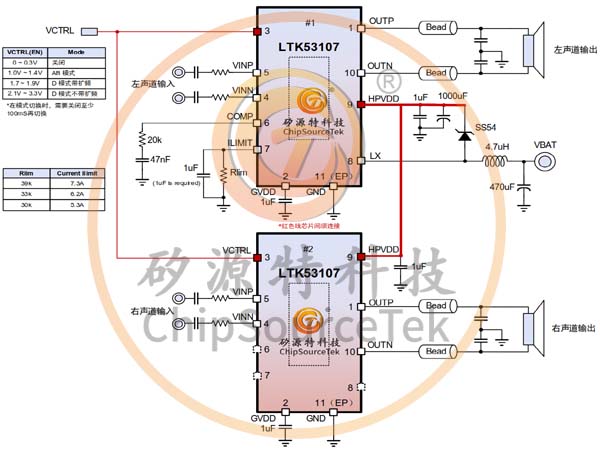
In order to better illustrate the application scheme, Fig.2 illustrates the combined implementation circuit of two LTK53107, #1 and #2, as follows:
The VCTRL (Pin3) of 1, #1, and #2 need to be connected together as the enable control pin of the entire system (can control AB, D switching, but need to pay attention to the mode
When switching, it is necessary to disable the enable function for at least 100mS, as shown in the figure.
2, #1 has a complete peripheral circuit (including booster supporting devices), boosted HPVDD, while directly connected to the HPVDD of #2 (Pin9).
3. Pin6, 7, and 8 of #2 are suspended without external devices.
4, the current capacity can be set by the Rlim resistance of the #1 ILIMIT pin, and it is usually not recommended to exceed 43kΩ.
5. The capacitor connected to ILIMIT is recommended to be greater than or equal to 1uF. It should be noted that too small the capacitor value will lead to a large starting current, which will cause damage to the system.

Electrical characteristic
VBAT=3.7V, AV=26dB, TA= 25oC (Typical case)
Performance parameter
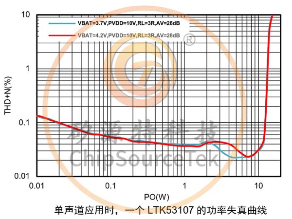
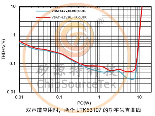
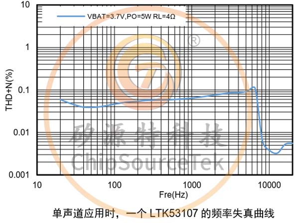
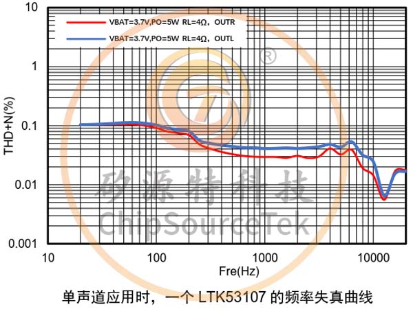
The LTK53107 delivers excellent distortion characteristics over the full frequency range in both mono and dual channel applications to meet customer power loss requirements


PCB guide
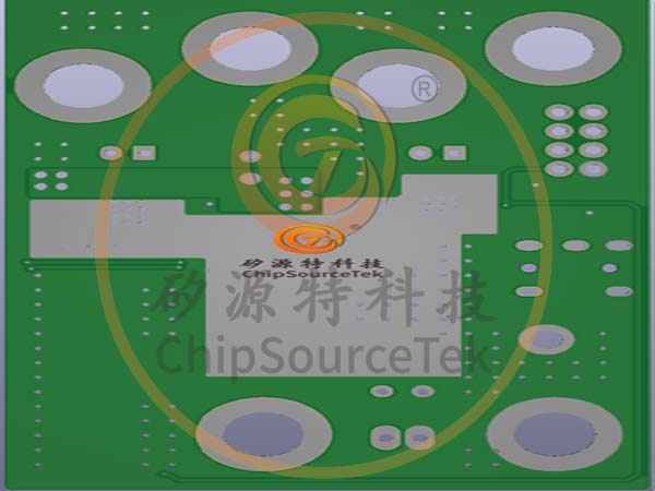
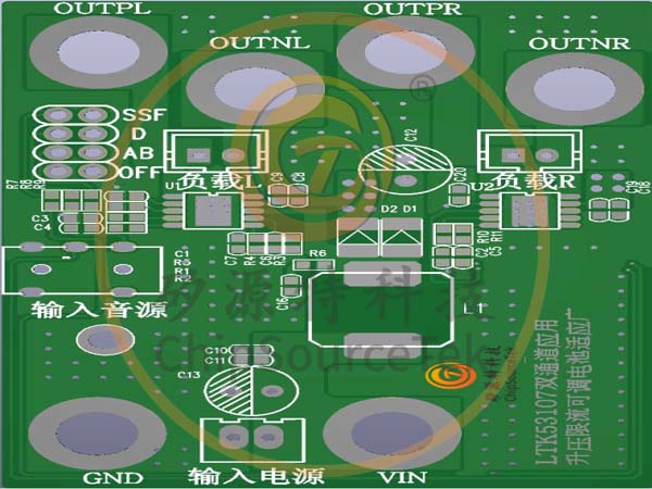
DEMO board top layer reference diagram

DEMO board bottom reference diagram
