Products
CST8250
The unique DRC (Dynamic range control) technology of the CST8250 reduces the distortion caused by waveform cutting during high-power output, and the dynamic response is better than that of similar products.
CST8250 can switch between headset mode and power amplifier mode. When the chip switches to headset mode, the internal circuit of the chip can drive the stereo headset, and the power amplifier mode can be switched to the stereo speaker.
The CST8250 is available in an eSOP10 package with heat sink.
CST8250 Description:
The CST8250 is a 2*8.0W dual-channel AB/D class stereo audio amplifier.
The CST8250's single-ended input architecture and extremely high PSRR effectively improve the CST8250's ability to suppress RF noise. The filter-free PWM modulation structure and gain built-in approach reduce external components, PCB area and system costs, and simplify design. Up to 90% efficiency, fast start-up time and small package size make the CST8250 the perfect choice for portable audio products. The unique DRC (Dynamic range control) technology of the CST8250 reduces the distortion caused by waveform cutting during high-power output, and the dynamic response is better than that of similar products.
CST8250 can switch between headset mode and power amplifier mode. When the chip switches to headset mode, the internal circuit of the chip can drive the stereo headset, and the power amplifier mode can be switched to the stereo speaker.
CST8250 also has a first-line pulse function, which can control a single pin to make the chip enter Class D, Class AB mode and off mode to achieve the purpose of saving IO port. CST8250 can completely eliminate EMI interference in Class AB mode. The CST8250 can withstand up to 7.0V.
The CST8250 has a very low turn-off current, which greatly extends the standby time of the system. OCP, OTP, UVLO protection enhances system reliability. Turning POP-click suppression on and off improves the auditory perception of the system and simplifies system debugging.
The CST8250 is available in an eSOP10 package with heat sink.
CST8250 Feature:
CST8250 Output power:
-2*8.0W (VDD=7.0V, RL=3Ω+15UH THD+N=10%)
-2*6.6W (VDD=7.0V, RL=4Ω+33UH THD+N=10%)
Operating voltage: 2.8V to 7.0V
Low distortion and noise
FM mode without interference
Comes with earphone switching mode
One-line pulse control
Enable or disable the POP-click suppression function
Turn-off current (<1uA)
OCP, OTP, and UVLO protection functions
The CST8250 is available in an eSOP10 package
CST8250 Applications:
Security monitoring system
Storyteller equipment
Smart door lock application
Portable audio equipment
megaphone
Card speakers, Blue tooth speakers, USB speakers
CST8250 Ordering Instructions:
Part No. | Package | Mark* | Tape/Reel |
CST8250 | eSOP10 | CST-LOGO-CST8250 XXXXXX | 4000颗/盘 |
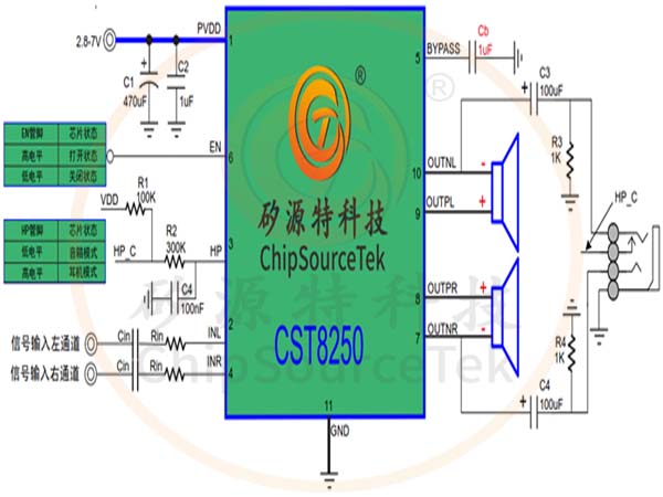
CST8250 Typical application schematic diagram:

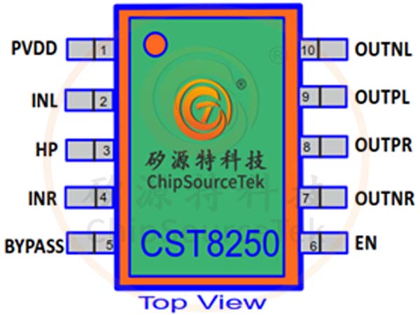
CST8250 pin diagram and pin description:
 | Number | Name | I/O | Pin Descripation |
1 | PVDD | I | Power supply positive terminal | |
2 | INL | I | Left channel input | |
3 | HP | I | Headset/speaker mode control, high level is headset mode, low level is speaker mode | |
4 | INR | I | Right channel input | |
5 | BYPASS | I | The internal analog reference source is connected to the bypass capacitor | |
 | 6 | EN | I | Chip off control, low level is off, high level is on. |
7 | OUTNR | O | Right channel reverse output | |
8 | OUTPR | O | Right channel forward output | |
9 | OUTPL | O | Left channel forward output | |
10 | OUTNR | O | Left channel reverse output | |
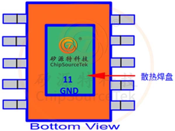
11 | GND | GND | The copper ground terminal at the bottom of the chip is exposed, and the power supply is negative |
CST8250 Recommended Working Conditions:
argument | symbol | Numerical value | unit |
Supply voltage | VDD | 3-6.7V | V |
Operating ambient temperature | TSTG | -40℃ to 85℃ | ℃ |
Junction temperature | TJ | - | ℃ |
CST8250 electrical characteristics: AV=20dB, TA=25℃, without special instructions, the project is tested at VDD=5V,4Ω+33uH conditions:
Description | symbol | Test condition | Minimum value | Typical value | Maximum value | unit | |
Static current | IDD | VDD =5V,D类 | - | 18 | 23 | mA | |
VDD =5V,AB类 |
| 20 | 24 | mA | |||
Turn-off current | ISHDN | VDD=3V to 5 V | - | 1 |
| uA | |
Static floor noise | Vn | VDD=5V ,AV=20DB,Awting |
| 130 |
| uV | |
Class D frequency | FSW | VDD=5V |
| 750 |
| kHz | |
Output offset voltage | Vos | VIN=0V |
| 10 |
| mV | |
Start-up time | Tstart | Vdd=5V,Bypass=1uF |
| 170 |
| ms | |
gain | Av | D类模式,RIN=27k |
| ≈20.5 |
| dB | |
Power off voltage | VddEN | EN=1 |
| <1.6 |
| V | |
Power supply opening voltage | Vddopen | EN=1 |
| >2.8 |
| V | |
EN Off voltage | VENEN |
|
| <0.7 |
| V | |
EN on voltage | VENopen |
|
| >1.3 |
| V | |
Class D opening voltage | MODE/D |
|
| <0.7 |
| V | |
Class AB on voltage | MODE/AB |
|
| >1.8 |
| V | |
Overtemperature protection | OTP |
|
| 180 |
| ℃ | |
Static on-resistance | RDSON | IDS=0.5A VGS=4.2V | P_MOSFET |
| 150 |
| mΩ |
N_MOSFET |
| 120 |
| ||||
Built-in input resistance | Rs |
|
| 7.5K |
| kΩ | |
Built-in feedback resistance | Rf |
|
| 185K |
| kΩ | |
efficiency | ηC |
|
| 90.3 |
| % | |
CSST8250 Class-D power: AV=20dB, TA=25℃, without special instructions, the project is tested under VDD=5V,4Ω :
argument | symbol | Test condition | Minimum value | Typical value | ximum value | unit | |
Output power |
Po | THD+N=10%, f=1kHz,RL=4Ω; | VDD=7V | - | 6.6 | - |
W |
VDD=6V | - | 4.9 | - | ||||
VDD=5V |
| 3.2 |
| ||||
VDD=4.2V |
| 2.2 |
| ||||
THD+N=10%, f=1kHz,RL=3Ω; | VDD=7V | - | 8.0 | - |
W | ||
VDD=6V |
| 5.6 |
| ||||
VDD=5V |
| 4.1 |
| ||||
VDD=4.2V | - | 2.9 | - | ||||
Total harmonic distortion plus noise | THD+N | VDD=5VPo=1W,RL=4Ω | f=1kHz | - | 0.08 | - | % |
CST8250 Limit parameters:
argument | symbol | value | unit |
供电电压 | VDD | 7V(MAX) | V |
存储温度 | TSTG | -65℃-150℃ | ℃ |
结温度 | TJ | 160℃ | ℃ |
CST8250 Characteristic curve Characteristic curve Test conditions (TA=25℃)
Description | Test condition | ID |
Input Amplitude VS. Output Amplitude | VDD=5V,RL=4Ω+33uH ,Class_D | Figure 1 |
Output Power VS. THD+N _Class_D | RL=3Ω+22uH,AV=20dB,Class_D | Figure 2 |
RL=4Ω+33uH,AV=20dB,Class_D | Figure 3 | |
Output Power VS.THD+N_Class_AB | RL=4Ω,AV=20dB , Class_AB | Figure 4 |
Frequency VS.THD+N | VDD=5V,RL=4 Ω,AV=20dB,Po=1W,Class_D_Awting | Figure 5 |
Input Voltage VS.Power Crrent | VDD=3.0V-5V,Class_D | Figure 6 |
Input Voltage VS. Maximum Output Power | RL=4Ω+33uH,THD=10%, Class_D | Figure 7 |
Frequency Response | VDD=5V,RL=4Ω,Class_D | Figure 8 |
CST8250 Application Information:
Power amplifier gain control: In Class D mode, the output is a (PWM signal) digital signal, and its gain can be adjusted by RIN.

AV is the gain, usually expressed in dB. The unit of the above calculation result is a multiple, 20Log multiple =dB.
AV is the gain, usually expressed in DB. The unit of the above calculation result is a multiple, 20Log multiple =dB.
The unit of RIN resistance is KΩ, 185KΩ is the internal feedback resistance (RF), and 7.5KΩ is the built-in series resistance (RS). RIN is defined by the user according to the actual supply voltage, input amplitude, and distortion degree. For example, RIN=27K, =10.5 times, AV=20.4DB
The input capacitance (CIN) and input resistance (RIN) constitute a high-pass filter whose cutoff frequency is:

When the Cin capacitance is selected to a small value, it can filter out low-frequency noise coupled from the input and help reduce POPO when turned on
EMI processing:For long output lines or close to sensitive devices, it is recommended to add magnetic beads and capacitors, which can effectively reduce EMI. The device is placed close to the chip
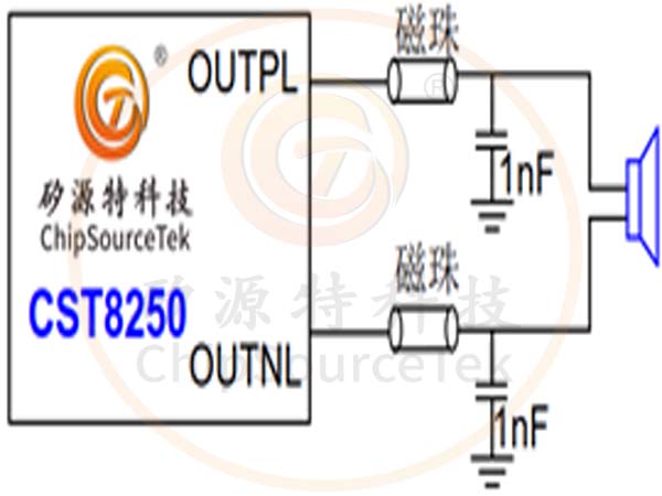
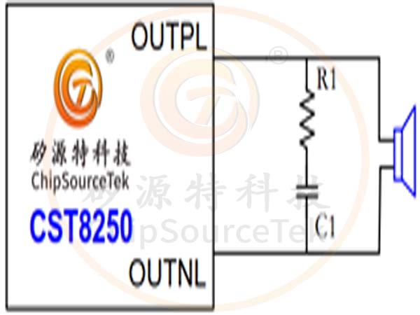
RC buffer circuit:If the horn load impedance value is small, it is recommended to have a resistor and a capacitor at the output end to absorb voltage spikes to prevent the chip from working abnormally. Resistance recommended: 2Ω-8Ω, capacitor recommended:500PF-10NF
EN pin control: The CST8250 can control Class AB and Class D mode switching by controlling the EN foot: The advantage of first-line pulse control is that it can save the main control IO, and you can switch multiple working modes of the power amplifier by using only one IO port.
EN pin software control (one-line pulse) : EN pin input different pulse signals switch power amplifier class AB, Class D mode.
1. The chip switches to Class D mode waveform:

2、The chip switches to Class AB mode waveform:

HP Mode control:When the HP pin is in high power mode, the chip is in headset mode and the output is single-ended. When the HP pin is in low power mode, the chip is in speaker mode
HP pin | Chip status |
High level | Headphone mode |
Low levelSpeaker mode |
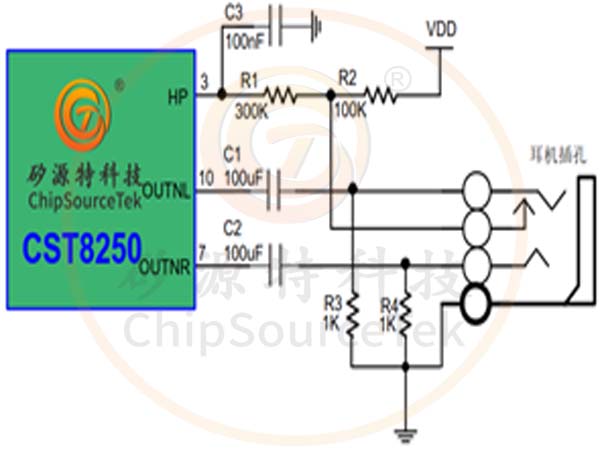
Above is a diagram of the headphone jack:
When no headphone is inserted, the HP foot divides voltage through R2 and R3, resulting in a low HP point potential and the chip operating in speaker mode.
When the headset is inserted, the internal short-circuit feet of the headset are separated, R2 and R3 no longer form a voltage divider, HP is high, the chip enters the headset mode, and the output is single-ended output.
Bypass capacitor: The Bypass capacitor is very important. The size of the Bypass capacitor determines the startup time of the power amplifier chip. The size of the bypass capacitor affects the power rejection ratio, noise, and POP performance of the chip. You are advised to set the capacitor to 1uF because the charging speed of the Bypass is slower than that at the input signal end, and the POP sound is smaller.
Overtemperature protection:The CST8250 has an overtemperature protection circuit to prevent device damage when the internal temperature exceeds 165 ° C. This value varies by 25 ° C between devices. When the internal circuit exceeds the set protection temperature, the device enters the off state and the output is cut off. When the temperature drops by 15 ° C, the device works normally again.
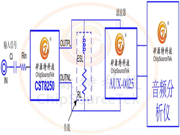
Test method: Filter test must be added when testing Class D mode. AUX-0025 is the filter. In order to test the data accurately and meet the practical application, an inductor is connected in series at the RL load end to simulate the parasitic inductor in the horn.
CST8250 PCB design considerations
Power supply pins (VDD, PVDDL, and PVDDR) should be as thick as possible. If holes must be drilled for power cables, use porous connections and increase the inner diameter of the holes. Do not use a single hole to connect power cables directly.
Input capacitance (Cin) and input resistance (Rin) are placed as close as possible to the pin of the power amplifier chip, and it is best to use the ground routing mode, which can effectively suppress the noise of other signal coupling.
Place the Bypass capacitor as close to the chip pin as possible.
It is recommended that the bottom heat sink of the CST8250 be welded to the PCB board for chip heat dissipation. It is recommended that the PCB use a large area of copper to connect the heat sink in the middle of the chip, and a certain range of copper exposure to help the chip heat dissipation.
The pin of the CST8250 output connecting to the horn should be as short as possible, and the width of the cable should be at least 0.4mm

