
Products
Products
CST8F005X
The CST8F005X series chip is an 8-bit microcontroller based on an enhanced 1T tiny 8051 core, with instructions fully compatible with traditional 8051 and running 10 times faster than traditional 8051. CST8F005X integrates 32KB Flash, 8KB programmable Boot Loader, 1.5KB SRAM, 26 channel TouchKey, 1 26 channel 12 bit precision ADC, software LED driver, 4 pairs of 8-channel 16 bit PWM with timer function, 3 general-purpose 16 bit timers, 2 UART, 1 I2C, 1 SPI, 32MHz internal RC oscillator, 32KHz internal RC oscillator, 32.768KHz external crystal oscillator, external high-speed oscillator, 26 GPIO and other resources.
CST8F005X Description:
The CST8F005X series chip is an 8-bit microcontroller based on an enhanced 1T tiny 8051 core, with instructions fully compatible with traditional 8051 and running 10 times faster than traditional 8051. CST8F005X integrates 32KB Flash, 8KB programmable Boot Loader, 1.5KB SRAM, 26 channel TouchKey, 1 26 channel 12 bit precision ADC, software LED driver、4 pairs of 8-channel 16 bit PWM with timer function, 3 universal 16 bit timers, 2 UART, 1 I2C, 1 SPI, 32MHz internal RC oscillator, 32KHz internal RC oscillator, 32.768KHZ external crystal oscillator, external high-speed oscillator, 26 GPIO and other resources. In order to improve chip reliability, CST8F005X also integrates power on/off reset, 8-level optional voltage low voltage detection (LVD), low-power independent watchdog counter (WDT), self wake-up timer (WKT) and other modules. CST8F005X has excellent anti-interference ability and low power consumption characteristics, making it very suitable for industrial control and consumer electronics fields such as home lighting, control switches, large and small household appliances, wireless communication, etc.
CST8F005X Main characteristics:
* Working voltage: 2.0V-5.5V
* Working temperature:- 40-+105℃
* Encapsulation type:
SSOP28L/QFN28/SSOP24L/QFN24/TSSOP20/QFN20
* Kernel: 1T tiny 8051
* Maximum operating frequency: 32MHz
* Flash ROM: 32K bytes, 100000 erasures
* Boot Loader: 8K bytes, 100000 erasures
* SRAM: Internal 256 bytes, External 1.5K bytes
* Clock( 3.3V@25 ℃)
- External high-speed crystal oscillator LOSC: 32.768KHZ
- External high-speed crystal oscillator HOSC: 2-32MHZ
- Built in RC oscillator LRC: 32KHz, adjustable accuracy ± 2%
- Built in RC oscillator HRC: 32MHz, adjustable accuracy ± 1%
* Interrupt
- 9 valid interrupt sources, two-level interrupt priority
- 6 external interrupts, configurable for any pin input, supporting up/down/dual edge triggering
* Timer
- 3 16 bit universal timers 0/1/2, compatible with standard 8051
* IO port
- 26 general-purpose GPIO ports
- Hold push-pull/open drain/pull-up/pull-down/high resistance modes, etc
- Pull up is 15K Ω, pull down is 15K Ω
- Push current 30mA@0.7VDD Inject current 80mA@0.3VDD
* Universal Serial Interface (UART)
- 2 UART interfaces: UART0 and UART1, compatible with standard 8051
- UART1 can choose any pin, and UART0/1 can adjust the duty cycle as desired
* SPI interface (SPI)
- Supports master-slave mode, three wire and four wire modes
- The maximum transmission and reception speed can reach 8MHz/bit (1/4 system clock)
* I2C Slave Interface (I2C)
- Built in 1 I2C interface, supports standard/fast mode
- Optional pin output
* Watchdog (WDT)
- 15 bit watchdog timer, counting clock is LRC clock
- 8-bit adjustment accuracy, with an adjustment range of 7.8125ms-1s
- Configurable watchdog generates reset or interrupt
* Self Wake Timer (WKT)
- Optional interrupt time is 1ms~1s, supports interrupt wake-up
- Optional external LOSC clock source, supporting 1-second precise timing
* Pulse Width Modulation (PWM)
- 4 pairs with 4-bit pre divided 12 bit PWM, optional clock source, can directly output clock, adjustable period and duty cycle, supports any pin output
- 3 pairs support timer counting capture function, complementary output and dead zone control
- 1 pair of multifunctional PWM, including edge alignment and center alignment modes, supporting complementary output and dead zone control, supporting braking and monostable power Can be used for square wave motor drive and industrial control
* Low Voltage Detection (LVD)
- Level 8 voltage detection 1.8/2.4/2.7/3.0/3.3/3.7/4.0/4.3V
- Low voltage reset or interrupt can be set
* Touch Key
- Up to 26 channels
- Support touch wake-up with low power consumption
- Can be tested through dynamic CS-10V and EFT-4KV
* High precision operational amplifier (OP)
- 1 high-precision operational amplifier that supports tuning
- Can be used alone or for amplifying the ADC front-end
* Analog to Digital Converter (ADC)
- 12 bit SAR ADC, with a total of 26 channels, supporting sampling at any pin
- Maximum conversion speed of 1MHz, supporting comparator function
- Built in 1/2 reference voltage channel, 1/2 VDD channel, VSS channel, and OP channel
- Built in 1.024/2.048/3.072/4.096V internal reference
* LED driver (LED)
- Support forward and backward LED scanning and matrix LED scanning
- SEG and COM can be selected with any pin, and the forward and backward LED scanning can achieve up to 25SEG * 26COM. The matrix supports 18SEG * 8COM
- Supports infinite duty cycle adjustment, which can perfectly solve the problem of uneven LED display with different colors and brightness
* Program download and simulation
- Support ISP and IAP, IAP can be configured in size
- Support online simulation function and program read protection
* Low power consumption
- IDLE mode minimum current 2.5uA
- STOP mode minimum current 2.5uA
- Internal LRC operating power consumption of 3.5uA
- 32Mhz@5V Operating with a typical power consumption of 2.5mA
* Anti-interference characteristics
- EFT>±4KV
- ESD HBM>±8KV
- Latch up>500mA
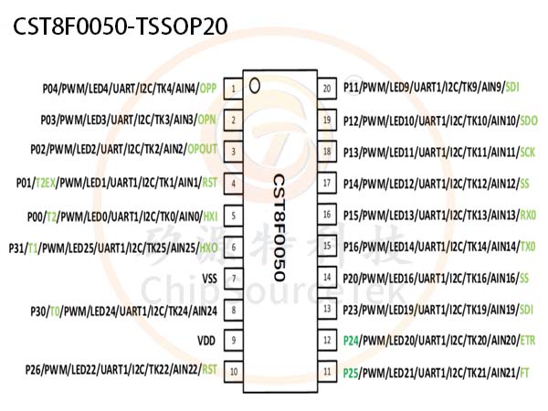
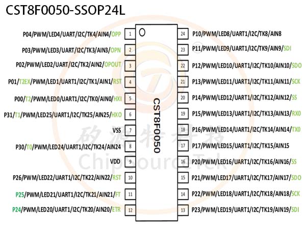
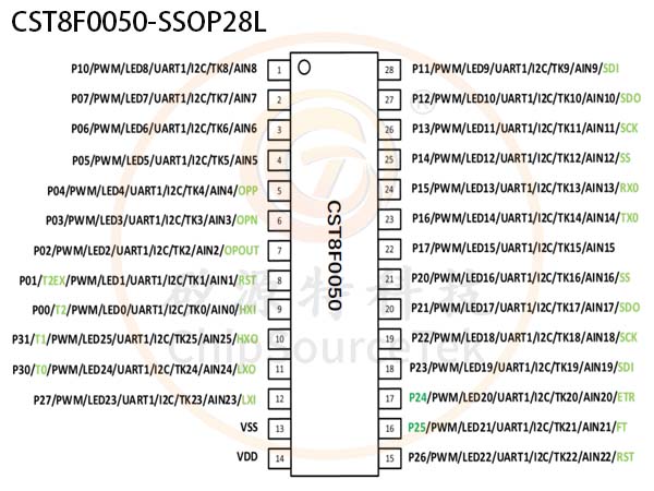
CST8F005X Encapsulation Definition:
The default simulation and burning ports are VDD, GND, P24 (SCL), and P25 (SDA). SCL and SDA can be modified to other IO settings as needed.
CST8F005X IO port (GPIO):
The CST8F005X series chip has 26 programmable multifunctional I/O ports in addition to power and ground ports, and its main features are as follows.
* Can be configured as high impedance mode
* The I/O structure can be independently configured with pull-up (≈ 18K Ω) and pull-down (≈ 18K Ω) settings
* Output mode can be selected as open drain output or push-pull output
* Data output latch supports read modify write operations
* Supports a wide voltage range of 2.0-5.5V
* When set as push-pull output, push current 35mA@0.7VDD Inject current 80mA@0.3VDD
* Can simultaneously turn on the up and down buttons, simulate the 1/2 BIAS driver of LCD, without the need for external resistors
The IO port structure diagram is shown in the following figure.
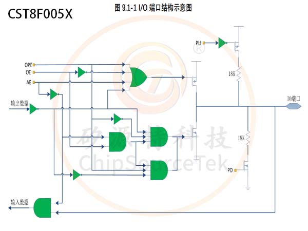
Remarks:
OPE: IO Port Open Leakage Enable Signal
OE: IO port output enable signal
AE: IO port simulation function enable signal
PU: IO port pull-up enable signal
PD: IO port pull-down enable signal
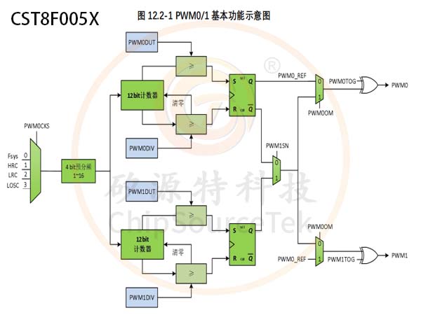
CST8F005X PWM Basic Function Diagram:
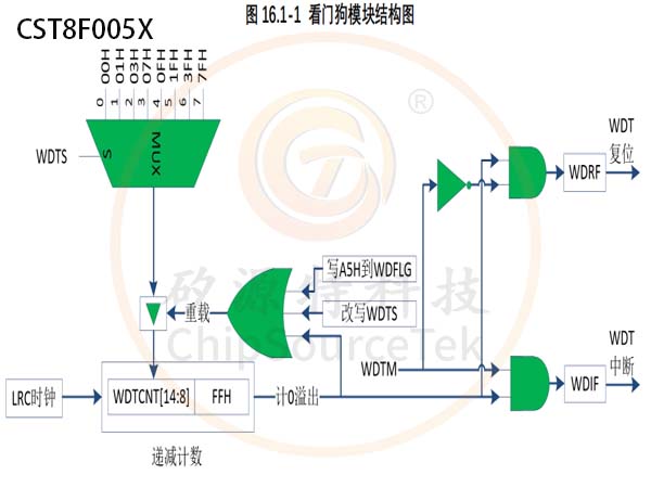
CST8F005X Structure diagram of watchdog module:
The CST8F005X series chip is an 8-bit microcontroller based on an enhanced 1T tiny 8051 core, with instructions fully compatible with traditional 8051 and running 10 times faster than traditional 8051. CST8F005X integrates 32KB Flash, 8KB programmable Boot Loader, 1.5KB SRAM, 26 channel TouchKey, 1 26 channel 12 bit precision ADC, software LED driver、4 pairs of 8-channel 16 bit PWM with timer function, 3 universal 16 bit timers, 2 UART, 1 I2C, 1 SPI, 32MHz internal RC oscillator, 32KHz internal RC oscillator, 32.768KHZ external crystal oscillator, external high-speed oscillator, 26 GPIO and other resources. In order to improve chip reliability, CST8F005X also integrates power on/off reset, 8-level optional voltage low voltage detection (LVD), low-power independent watchdog counter (WDT), self wake-up timer (WKT) and other modules. CST8F005X has excellent anti-interference ability and low power consumption characteristics, making it very suitable for industrial control and consumer electronics fields such as home lighting, control switches, large and small household appliances, wireless communication, etc.
CST8F005X Main characteristics:
* Working voltage: 2.0V-5.5V
* Working temperature:- 40-+105℃
* Encapsulation type:
SSOP28L/QFN28/SSOP24L/QFN24/TSSOP20/QFN20
* Kernel: 1T tiny 8051
* Maximum operating frequency: 32MHz
* Flash ROM: 32K bytes, 100000 erasures
* Boot Loader: 8K bytes, 100000 erasures
* SRAM: Internal 256 bytes, External 1.5K bytes
* Clock( 3.3V@25 ℃)
- External high-speed crystal oscillator LOSC: 32.768KHZ
- External high-speed crystal oscillator HOSC: 2-32MHZ
- Built in RC oscillator LRC: 32KHz, adjustable accuracy ± 2%
- Built in RC oscillator HRC: 32MHz, adjustable accuracy ± 1%
* Interrupt
- 9 valid interrupt sources, two-level interrupt priority
- 6 external interrupts, configurable for any pin input, supporting up/down/dual edge triggering
* Timer
- 3 16 bit universal timers 0/1/2, compatible with standard 8051
* IO port
- 26 general-purpose GPIO ports
- Hold push-pull/open drain/pull-up/pull-down/high resistance modes, etc
- Pull up is 15K Ω, pull down is 15K Ω
- Push current 30mA@0.7VDD Inject current 80mA@0.3VDD
* Universal Serial Interface (UART)
- 2 UART interfaces: UART0 and UART1, compatible with standard 8051
- UART1 can choose any pin, and UART0/1 can adjust the duty cycle as desired
* SPI interface (SPI)
- Supports master-slave mode, three wire and four wire modes
- The maximum transmission and reception speed can reach 8MHz/bit (1/4 system clock)
* I2C Slave Interface (I2C)
- Built in 1 I2C interface, supports standard/fast mode
- Optional pin output
* Watchdog (WDT)
- 15 bit watchdog timer, counting clock is LRC clock
- 8-bit adjustment accuracy, with an adjustment range of 7.8125ms-1s
- Configurable watchdog generates reset or interrupt
* Self Wake Timer (WKT)
- Optional interrupt time is 1ms~1s, supports interrupt wake-up
- Optional external LOSC clock source, supporting 1-second precise timing
* Pulse Width Modulation (PWM)
- 4 pairs with 4-bit pre divided 12 bit PWM, optional clock source, can directly output clock, adjustable period and duty cycle, supports any pin output
- 3 pairs support timer counting capture function, complementary output and dead zone control
- 1 pair of multifunctional PWM, including edge alignment and center alignment modes, supporting complementary output and dead zone control, supporting braking and monostable power Can be used for square wave motor drive and industrial control
* Low Voltage Detection (LVD)
- Level 8 voltage detection 1.8/2.4/2.7/3.0/3.3/3.7/4.0/4.3V
- Low voltage reset or interrupt can be set
* Touch Key
- Up to 26 channels
- Support touch wake-up with low power consumption
- Can be tested through dynamic CS-10V and EFT-4KV
* High precision operational amplifier (OP)
- 1 high-precision operational amplifier that supports tuning
- Can be used alone or for amplifying the ADC front-end
* Analog to Digital Converter (ADC)
- 12 bit SAR ADC, with a total of 26 channels, supporting sampling at any pin
- Maximum conversion speed of 1MHz, supporting comparator function
- Built in 1/2 reference voltage channel, 1/2 VDD channel, VSS channel, and OP channel
- Built in 1.024/2.048/3.072/4.096V internal reference
* LED driver (LED)
- Support forward and backward LED scanning and matrix LED scanning
- SEG and COM can be selected with any pin, and the forward and backward LED scanning can achieve up to 25SEG * 26COM. The matrix supports 18SEG * 8COM
- Supports infinite duty cycle adjustment, which can perfectly solve the problem of uneven LED display with different colors and brightness
* Program download and simulation
- Support ISP and IAP, IAP can be configured in size
- Support online simulation function and program read protection
* Low power consumption
- IDLE mode minimum current 2.5uA
- STOP mode minimum current 2.5uA
- Internal LRC operating power consumption of 3.5uA
- 32Mhz@5V Operating with a typical power consumption of 2.5mA
* Anti-interference characteristics
- EFT>±4KV
- ESD HBM>±8KV
- Latch up>500mA
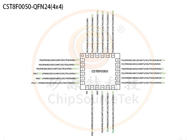
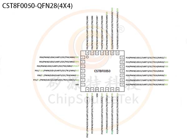
CST8F005X Encapsulation Definition:
The default simulation and burning ports are VDD, GND, P24 (SCL), and P25 (SDA). SCL and SDA can be modified to other IO settings as needed.
CST8F005X Ordering Information:
Product Name | Package | Unit quantity | Pack | Description |
CST8F0050T20U | TSSOP20 | 72/Tube, 14.4K/Box, 57.6K/Box | Tube | Main sales models |
CST8F0050P24U | SSOP24L | 50/Tube, 10K/Box, 100K/Box | Tube | Main sales models |
CST8F0050P28U | SSOP28L | 50/tube, 10K/box, 40K/box | Tube | Main sales models |
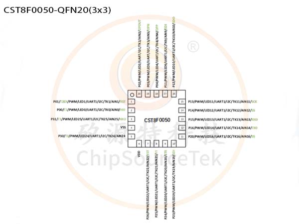
CST8F0050Q20T | QFN20(3X3) | 5K/Plate, 25K/Box, 100K/Box | Braid | Main sales models |
CST8F0050Q24T | QFN24(4X4) | 5K/Plate, 25K/Box, 100K/Box | Braid | Main sales models |
CST8F0050Q28T | QFN28(4X4) | 5K/Plate, 25K/Box, 100K/Box | Braid | Main sales models |
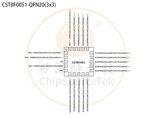
CST8F0051Q20T | QFN20(3X3) | 5K/Plate, 25K/Box, 100K/Box | Braid | Compatible models |
CST8F005X IO port (GPIO):
The CST8F005X series chip has 26 programmable multifunctional I/O ports in addition to power and ground ports, and its main features are as follows.
* Can be configured as high impedance mode
* The I/O structure can be independently configured with pull-up (≈ 18K Ω) and pull-down (≈ 18K Ω) settings
* Output mode can be selected as open drain output or push-pull output
* Data output latch supports read modify write operations
* Supports a wide voltage range of 2.0-5.5V
* When set as push-pull output, push current 35mA@0.7VDD Inject current 80mA@0.3VDD
* Can simultaneously turn on the up and down buttons, simulate the 1/2 BIAS driver of LCD, without the need for external resistors
The IO port structure diagram is shown in the following figure.
Remarks:
OPE: IO Port Open Leakage Enable Signal
OE: IO port output enable signal
AE: IO port simulation function enable signal
PU: IO port pull-up enable signal
PD: IO port pull-down enable signal
CST8F005X PWM Basic Function Diagram:
CST8F005X Structure diagram of watchdog module:

Please submit your basic information, send an email to Sales@ChipSourceTek.com, or call us at 13823761625 (same number as WeChat), and we will contact you as soon as possible!

WeChat Official Account

WeChat Service
 Email
Email QQ
QQ 13823761625
