
Products
Products


CST3240
CST3240 series multi-point capacitive touch chip, support single layer, multi-layer module and a variety of patterns, using multi-channel 7V high voltage drive, to achieve high performance, high sensitivity real multi-finger touch effect. Compared with the traditional single-channel low-voltage drive, it can provide higher signal-to-noise ratio and anti-interference ability. At the same time, the internal self-mutual capacitive sensing module, combined with intelligent scanning algorithm, has excellent anti-noise, waterproof and low power performance while realizing fast response.
CST3240 Description:
CST3240 series multi-point capacitive touch chip, support single layer, multi-layer module and a variety of patterns, using multi-channel 7V high voltage drive, to achieve high performance, high sensitivity real multi-finger touch effect. Compared with the traditional single-channel low-voltage drive, it can provide higher signal-to-noise ratio and anti-interference ability. At the same time, the internal self-mutual capacitive sensing module, combined with intelligent scanning algorithm, has excellent anti-noise, waterproof and low power performance while realizing fast response.
CST3240 Features:
High performance capacitance detection circuit and DSP module
Self-mutual integrated detection module;
Multi-channel high voltage drive at the same time, to achieve high sensitivity, high SNR sampling;
Dynamic wide range frequency hopping technology, support stronger anti-jamming ability;
Support passive capacitive touch pen;
Support standby gesture wake up function;
Support online programming;
Built-in watchdog;
Multiple key support.
Performance index
Typical refresh rate 100Hz;
With water operation, thumb recognition and big palm suppression;
Typical power consumption in dynamic mode: 10mA;
Typical power consumption in monitoring mode: 4mA (30Hz).
Typical power consumption in sleep mode: 20uA.
With water operation, thumb recognition and big palm suppression;
Typical power consumption in dynamic mode: 10mA;
Typical power consumption in monitoring mode: 4mA (30Hz).
Typical power consumption in sleep mode: 20uA.
Capacitive panel support
Supports up to 40 drive/sensing channels, and supports TX/RX interchanges;
Channel suspension/pull-down design support;
Support traditional DITO and SITO and various patterns;
Module parameters automatically adjust, the maximum support impedance up to 60K;
Cover Lens Thickness support, glass <= 2mm acrylic <=1mm.
Channel suspension/pull-down design support;
Support traditional DITO and SITO and various patterns;
Module parameters automatically adjust, the maximum support impedance up to 60K;
Cover Lens Thickness support, glass <= 2mm acrylic <=1mm.
Communication interface
2C master/slave communication interface, speed 50Khz~400Khz configurable;
GPIO support, a variety of working modes can be configured, built-in pull-up resistance mode;
Built-in 1.8V LDO, compatible with 1.8V/VDDA interface level can be matched.
GPIO support, a variety of working modes can be configured, built-in pull-up resistance mode;
Built-in 1.8V LDO, compatible with 1.8V/VDDA interface level can be matched.
Mains supply
Single power supply 2.8~3.6V, please refer to the circuit design, power ripple <=50mv; A small number of peripheral devices.
Package type: QFN52L 6 x 6
Package type: QFN52L 6 x 6
CST3240 Application:
Mobile phones, tablets, laptops, touchpads, etc.
CST3240 Typical application circuit diagram:
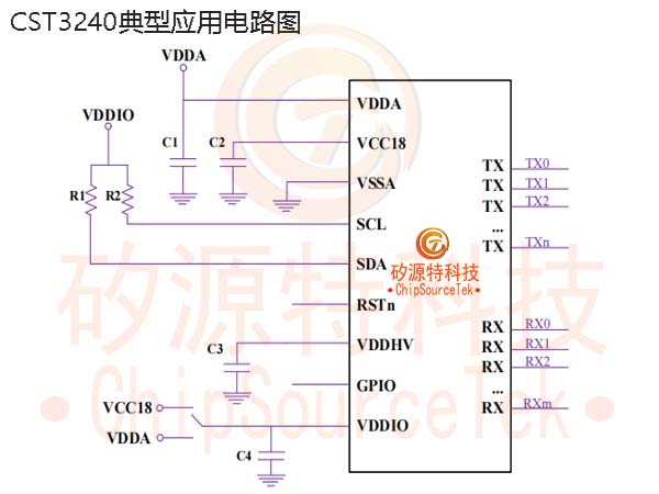
C1:2.2uF/10V C2: 1uF/10V
C3:100nF/10V C4: 1uF/10V
VDDIO: VDDA or VCC18, depending on IIC, SPI communication and RSTn voltage.
R1/R2: a pull-up resistor on the I2C bus, or an internal 5K pull-up resistor can be configured instead.
GPIO: can be used as an INT or SensorID to configure suspension or connect to GND.
C3:100nF/10V C4: 1uF/10V
VDDIO: VDDA or VCC18, depending on IIC, SPI communication and RSTn voltage.
R1/R2: a pull-up resistor on the I2C bus, or an internal 5K pull-up resistor can be configured instead.
GPIO: can be used as an INT or SensorID to configure suspension or connect to GND.
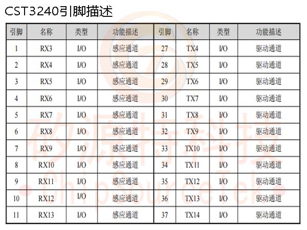
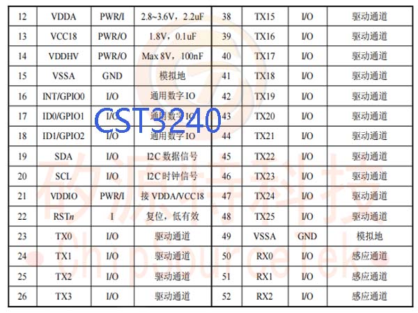
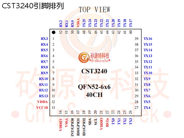
CST3240 Pin arrangement:
CST3240 Pin Description:


CST3240 Ordering Information:
CST3240 Ordering Information:
Part number (P/N) | encapsulation | Surface printing | package |
CST3240 | QFN52L 6*6 | CST3240 XXXXX (Production tracking code) | 4000/ disk, braided shipment |
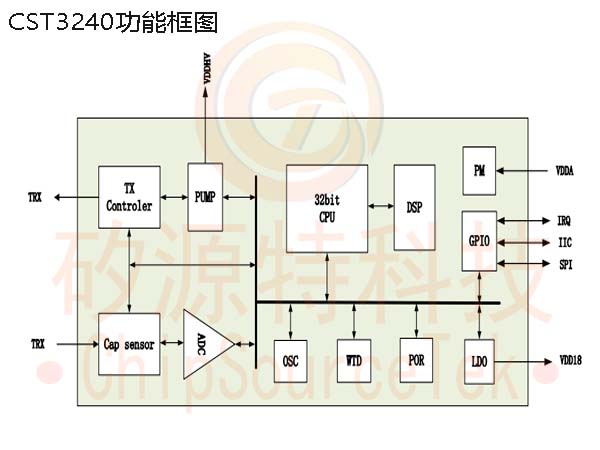
CST3240 function block diagram:


Please submit your basic information, send an email to Sales@ChipSourceTek.com, or call us at 13823761625 (same number as WeChat), and we will contact you as soon as possible!

WeChat Official Account

WeChat Service
 Email
Email QQ
QQ 13823761625
