
Products
Products
TRSP(M)5182A/5171A/5171S1/5086A
The TRSP(M)5182A/5171A/ 51711/5086A series are 4-bit microcontrollers that can play 4-channel melodies or 4-channel ADPCM. The TRSP series is OTP (one-time programmable) type memory, and the TRSM series is MASK type memory. The resolution of PWM is 8/10/12 bits.
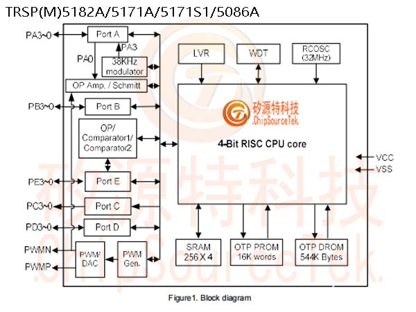
They include a low-cost, high-performance CMOS microprocessor. The clock frequency of this rise is usually 8.192 (±3%) MHz. The chip can operate in a wide voltage range from 2.0V to 5.5V. It contains program ROM (PROM) and data ROM (DROM) internally. The maximum program ROM (PROM) is 16K words and the maximum data ROM (DROM) size is 544K bytes. The maximum working SRAM is (256+2) notch. It provides a total of 16 software-programmable I/O ports and 4 outputs (defined by options).
They include a low-cost, high-performance CMOS microprocessor. The clock frequency of this rise is usually 8.192 (±3%) MHz. The chip can operate in a wide voltage range from 2.0V to 5.5V. It contains program ROM (PROM) and data ROM (DROM) internally. The maximum program ROM (PROM) is 16K words and the maximum data ROM (DROM) size is 544K bytes. The maximum working SRAM is (256+2) notch. It provides a total of 16 software-programmable I/O ports and 4 outputs (defined by options).
TRSP(M)5182A/5171A/ 51711/5086A General Description:
The TRSP(M)5182A/5171A/ 51711/5086A series are 4-bit microcontrollers that can play 4-channel melodies or 4-channel ADPCM. The TRSP series is OTP (one-time programmable) type memory, and the TRSM series is MASK type memory. The resolution of PWM is 8/10/12 bits.
They include a low-cost, high-performance CMOS microprocessor. The clock frequency of this rise is usually 8.192 (±3%) MHz. The chip can operate in a wide voltage range from 2.0V to 5.5V. It contains program ROM (PROM) and data ROM (DROM) internally. The maximum program ROM (PROM) is 16K words and the maximum data ROM (DROM) size is 544K bytes. The maximum working SRAM is (256+2) notch. It provides a total of 16 software-programmable I/O ports and 4 outputs (defined by options).
They include a low-cost, high-performance CMOS microprocessor. The clock frequency of this rise is usually 8.192 (±3%) MHz. The chip can operate in a wide voltage range from 2.0V to 5.5V. It contains program ROM (PROM) and data ROM (DROM) internally. The maximum program ROM (PROM) is 16K words and the maximum data ROM (DROM) size is 544K bytes. The maximum working SRAM is (256+2) notch. It provides a total of 16 software-programmable I/O ports and 4 outputs (defined by options).
TRSP(M)5182A/5171A/ 51711/5086A Features:
Operating voltage: 2.0V to 5.5V
MCU operating frequency: 8.192MHz
Memory size
- Program ROM size: Maximum 16K* 12-bit OTP type
- Data ROM size: Maximum 544K x 8-bit OTP type
-SRAM size: 256 x 4 bits
- User register: 2 x 4 bits
Wake up function in power off mode:
-HALT mode Wake up source: Ports A, B, D, and E can wake up from HALT mode to normal mode and execute wake up subroutines.
12 input/output pins: Ports A, B, and D can be defined individually as input or output ports.
4 Output pin: Port C.
Options for 4 input/output or 4 input pin definitions: If input pins are used, port E is defined as the input port. If input/output pins are selected, port E is defined as the input or output port.
Four reset conditions:
- Low pressure reset.
- Power on reset.
- External reset pin. (Low activity)
- Watchdog timer overflowed.
An internal interrupt source:
-PWM is interrupted.
WDT
- Watchdog timer, an option that can be enabled/disabled.
- The WDT period is 256 x 256 x 16/Fsys. (System clock=8.192MHz WDT period is 0.13 seconds)
Audio output:
- Support PWM or DAC mode options. (DAC functionality for TRSP series only)
- Support 8/10/12 bits.
Support options are set to pull-down resistance 1M, 50K or 220K ohm, reset pin (PB3 or PC3), low voltage reset, etc.
Oscillator fuse option ±3%, temperature and voltage compensation.
Support for read suppression of security options (1 bit).
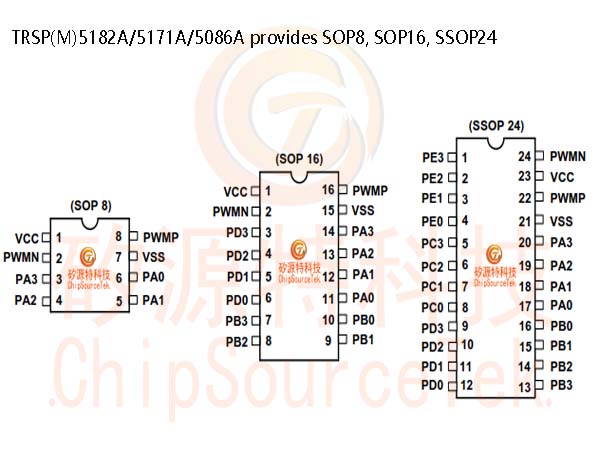
TRSP(M)5182A/5171A/ 51711/5086A package:
TRSP(M)5182A/5171A/ 51711/5086A block diagram:
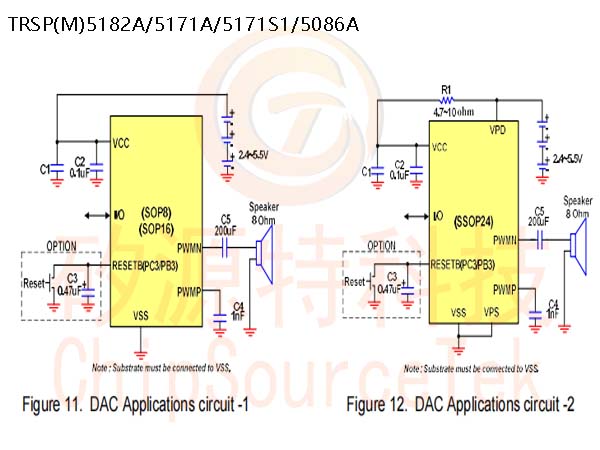
TRSP(M)5182A/5171A/ 51711/5086A Application circuit:

The DAC is selected by option
Attention:
1. For recording or remote car applications, please refer to the application instructions on the website.
2. C1: 47uF ~ 100uF (depending on application), C2: 0.1uF
3. For DAC applications, please refer to the application instructions on the website.
1. For recording or remote car applications, please refer to the application instructions on the website.
2. C1: 47uF ~ 100uF (depending on application), C2: 0.1uF
3. For DAC applications, please refer to the application instructions on the website.

Please submit your basic information, send an email to Sales@ChipSourceTek.com, or call us at 13823761625 (same number as WeChat), and we will contact you as soon as possible!

WeChat Official Account

WeChat Service
 Email
Email QQ
QQ 13823761625
