
Products
Products
NY8LP05A
The NY8LP05A is a high-performance 8-bit 65C02 microcontroller with LCD driver and Buzzer playback, three sets of 8-bit timer/counter, and 16 I/ OS. The ROM is an embedded EPROM architecture OTP IC(One Time Programmable).
MCU for CISC architecture is easy to program and control and plan for a variety of applications. In addition, it provides a variety of working modes Slow mode, Standby mode and Halt mode (Sleep Mode) to effectively reduce power consumption.
MCU for CISC architecture is easy to program and control and plan for a variety of applications. In addition, it provides a variety of working modes Slow mode, Standby mode and Halt mode (Sleep Mode) to effectively reduce power consumption.
NY8LP05A Description:
The NY8LP05A is a high-performance 8-bit 65C02 microcontroller with LCD driver and Buzzer playback, three sets of 8-bit timer/counter, and 16 I/ OS. The ROM is an embedded EPROM architecture OTP IC(One Time Programmable).
MCU for CISC architecture is easy to program and control and plan for a variety of applications. In addition, it provides a variety of working modes Slow mode, Standby mode and Halt mode (Sleep Mode) to effectively reduce power consumption.
MCU for CISC architecture is easy to program and control and plan for a variety of applications. In addition, it provides a variety of working modes Slow mode, Standby mode and Halt mode (Sleep Mode) to effectively reduce power consumption.
NY8LP05A Features:
Wide operating voltage range:
1.5V application, 1.1V~ 3.6V@ System clock ≤ 500KHz;
For 3.0V applications, 1.8V to 3.6 V@ System clock ≤ 4MHz.
4K-Byte OTP ROM.
64-Byte RAM.
LCD points (COM x SEG) : 4 x 15.
16 GPIO, 6 of which are shared with LCD SEG.
Dual pulse oscillation: The system clock can freely choose high or low speed.
High speed oscillation: IOSC4M/IOSC2M/IOSC500K.
Low-speed oscillation: IOSC32K/XTAL32K.
Built-in high precision oscillation line (+/ -1.5%).
Four operating modes can effectively save power and reduce power consumption:
Normal mode, Slow mode, Standby mode, and Halt mode.
In Normal mode, the CPU clock speed can be programmed:
Can be set to high speed oscillation 1/1, 1/2, 1/4, 1/8, 1/16, 1/32, 1/64, 1/128.
3 sets of 8-bit timers for applications such as 1-channel or 2-channel Buzzer or RFC.
Support for most LCD displays:
1/2, 1/3 bias.
1/2, 1/3, 1/4 duty.
A voltage bias circuit with built-in Charge pump boost or R-Bias resistor partial voltage is supplied for LCD display.
Internal RC oscillator mode for single-cell applications with a minimum LCD frame rate of 42Hz.
RFC function for temperature and humidity detection applications.
Complete system protection, Watchdog reset function and external reset pin.
Built-in low voltage detection of 1.05V/1.15V/1.25V/1.3V(1.5V application) or 1.75V/1.85V/1.95V/2.00V(3V application).
Diverse I/Os Settings: floating input, pull-low input, CMOS output, open-drain output.
1 or 2 channel Buzzer.
6 interrupt modes.
LCD point combination:
COMMON | SEGMENT | DOTS |
4 | 15 | 60 |
3 | 16 | 48 |
2 | 16 | 32 |
NY8LP05A BLOCK DIAGRAM:
.jpg)
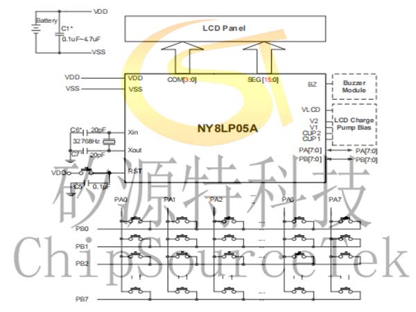
NY8LP05A APPLICATION CIRCUITS:
Application Circuit
PCB Layout Guidelines:
1. VDD must be connected to power input port directly, not the branch of each other.
2. VLCD should be higher than or equal to VDD, otherwise will cause large current.
3. VSS must be connected to ground input directly, not the branch of each other.
4. Capacitor (used for XTAL32K) is proposed to be 12~20 pF.
5. C1 is suggested 0.1uF~4.7uF.
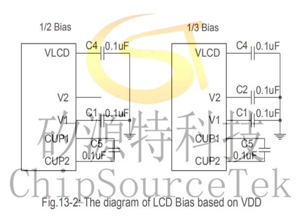
LCD ChargePump Bias (VDD for VLCD/V2/V1)
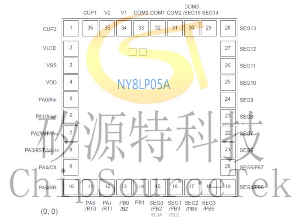
NY8LP05A DIE PAD DIAGRAM:

Please submit your basic information, send an email to Sales@ChipSourceTek.com, or call us at 13823761625 (same number as WeChat), and we will contact you as soon as possible!

WeChat Official Account

WeChat Service
 Email
Email QQ
QQ 13823761625
