
Products
Products
XM004
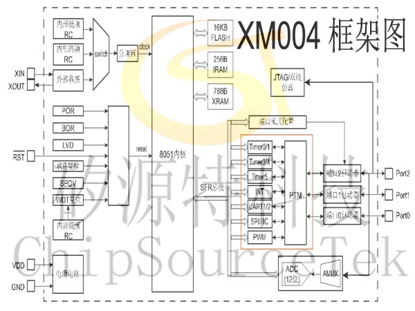
XM004 is a high speed and low power CMOS technology design and development of enhanced 8-bit MCU, internal 16K Bytes FLASH program memory, 256 Bytes IRAM and 768 Bytes XRAM, up to 18 bidirectional I/O ports. 1 peripheral function pin full mapping module PTM, 5 16-bit timers/counters, 3 sets of 16-bit dead zone control complementary PWM, 1 8-bit PWM, 2 UART, 1 SPI, 1 IIC, 16 external interrupts, 11+2 12-bit ADCs, Four system operating modes (normal, Low frequency, power down, and idle) and 17 interrupt sources.
XM004 Product Description:
XM004 is a high speed and low power CMOS technology design and development of enhanced 8-bit MCU, internal 16K Bytes FLASH program memory, 256 Bytes IRAM and 768 Bytes XRAM, up to 18 bidirectional I/O ports. 1 peripheral function pin full mapping module PTM, 5 16-bit timers/counters, 3 sets of 16-bit dead zone control complementary PWM, 1 8-bit PWM, 2 UART, 1 SPI, 1 IIC, 16 external interrupts, 11+2 12-bit ADCs, Four system operating modes (normal, Low frequency, power down, and idle) and 17 interrupt sources.
XM004 Features:
CPU
Enhanced 1T 8051 core
ROM
16K Bytes FLASH
IAP and ICP operations
Flexible code protection mode
RAM
256 Bytes IRAM
768 Bytes XRAM
clock
Internal high precision 32MHz RC
Internal 44KHz RC
External high frequency crystal oscillator 4MHz-20MHz
External low frequency crystal oscillator 32.768KHz
Multiple clock output
Multiple reset modes
Power-on reset (POR)
Multistage low voltage reset (BOR) - 4.2/3.9/3.6/3.0/2.6/2.4/2.0/1.8 V
Watchdog (WDT) reset
Software reset
Stack overflow reset
External pin low reset
External pin voltage (1.2V) detects reset
I/O
Up to 18 bidirectional I/O ports
A variety of modes can be configured: input, tape pull input, tape pull down input, Schmidt input, analog input, strong push-pull output, open leakage output, open leakage tape pull output. Peripheral function pin full mapping module PTM
interrupt
17 interrupt sources
Level 4 Interrupt priority
16 external interrupts
Timer/counter
T0/T1 compatible standard 8051, 16-bit automatic reload
T3 can work in power off mode
T4 can trigger timing using external signals
T5 with capture function
PWM
Up to 3 sets of 16-bit dead-zone control complementary PWM
- Supports six independent outputs
- Can be used as timer
- With fault detection function
- Border alignment or center alignment can be configured
1 channel 8-bit single output PWM
Communication module
2 UART
1 SPI
One IIC
ADC detection circuit
Supports 11+2 ch 12-bit ADC detection
ADC reference voltage can be selected internal VREF, external VREF, VDD
Low voltage detection module
VDD multi-stage voltage detection, interruptible 2.0/1.9-4.2/3.9/3.6/3.0/2.6/2.4 / V
Cyclic redundancy check (CRC)
Power saving mode
Idle mode
Power off mode
Working condition
Wide voltage 2.0V ~ 5.5V
Temperature range -40°C to +85°C
Package type
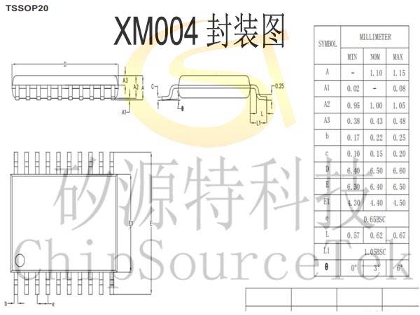
TSSOP20
XM004 Use precautions:
1. In order to ensure the stability of the system, there must be an indirect capacitance (the capacitance value must be equal to or greater than 0.1μF) in VDD and GND.
2. When the ADC module is used, when the internal reference voltage is 2V, the VDD voltage must be higher than 2.7V; when the internal reference voltage is 3/4V, the VDD must be higher than the internal reference voltage of 0.5V.
3. When the system is performing IAP operations, the CPU enters idle mode and does not respond to any interruption.
4. P2.7 pins are reset pins by default before delivery. You can configure this port as an ordinary IO pin by using the configuration code option.
5. Before IAP erase and enter power down mode, the FREQ_CLK register needs to be configured to indicate the current CPU clock frequency.
Enhanced 1T 8051 core
ROM
16K Bytes FLASH
IAP and ICP operations
Flexible code protection mode
RAM
256 Bytes IRAM
768 Bytes XRAM
clock
Internal high precision 32MHz RC
Internal 44KHz RC
External high frequency crystal oscillator 4MHz-20MHz
External low frequency crystal oscillator 32.768KHz
Multiple clock output
Multiple reset modes
Power-on reset (POR)
Multistage low voltage reset (BOR) - 4.2/3.9/3.6/3.0/2.6/2.4/2.0/1.8 V
Watchdog (WDT) reset
Software reset
Stack overflow reset
External pin low reset
External pin voltage (1.2V) detects reset
I/O
Up to 18 bidirectional I/O ports
A variety of modes can be configured: input, tape pull input, tape pull down input, Schmidt input, analog input, strong push-pull output, open leakage output, open leakage tape pull output. Peripheral function pin full mapping module PTM
interrupt
17 interrupt sources
Level 4 Interrupt priority
16 external interrupts
Timer/counter
T0/T1 compatible standard 8051, 16-bit automatic reload
T3 can work in power off mode
T4 can trigger timing using external signals
T5 with capture function
PWM
Up to 3 sets of 16-bit dead-zone control complementary PWM
- Supports six independent outputs
- Can be used as timer
- With fault detection function
- Border alignment or center alignment can be configured
1 channel 8-bit single output PWM
Communication module
2 UART
1 SPI
One IIC
ADC detection circuit
Supports 11+2 ch 12-bit ADC detection
ADC reference voltage can be selected internal VREF, external VREF, VDD
Low voltage detection module
VDD multi-stage voltage detection, interruptible 2.0/1.9-4.2/3.9/3.6/3.0/2.6/2.4 / V
Cyclic redundancy check (CRC)
Power saving mode
Idle mode
Power off mode
Working condition
Wide voltage 2.0V ~ 5.5V
Temperature range -40°C to +85°C
Package type
TSSOP20
XM004 Use precautions:
1. In order to ensure the stability of the system, there must be an indirect capacitance (the capacitance value must be equal to or greater than 0.1μF) in VDD and GND.
2. When the ADC module is used, when the internal reference voltage is 2V, the VDD voltage must be higher than 2.7V; when the internal reference voltage is 3/4V, the VDD must be higher than the internal reference voltage of 0.5V.
3. When the system is performing IAP operations, the CPU enters idle mode and does not respond to any interruption.
4. P2.7 pins are reset pins by default before delivery. You can configure this port as an ordinary IO pin by using the configuration code option.
5. Before IAP erase and enter power down mode, the FREQ_CLK register needs to be configured to indicate the current CPU clock frequency.
XM004 System block diagram:
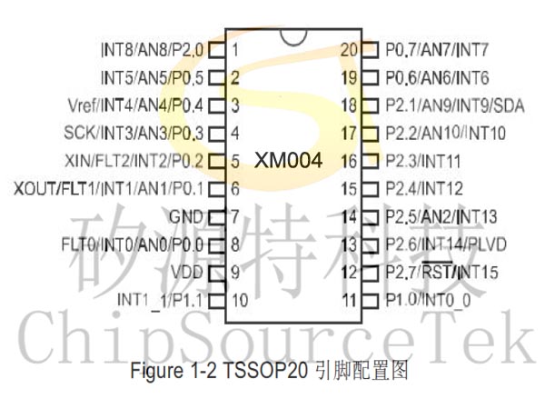
XM004 Pin configuration and description:
XM004 package diagram:
Peripheral function pin full mapping module PTM
The built-in peripheral Function Pin Full Mapping module (PTM) of the XM004 allows most peripheral function pins to be configured on any non-power port (VDD, GND) through user software operation.
PTM module features
When the peripheral pin is an input function (T0/1/3/5 external input, RXD, etc.) feature, the system will allow its many-to-one mapping, that is, multiple input feature peripheral function pins are assigned to the same IO port, which can better optimize the user system.
When the peripheral pins are output functions (T0/1/4 clock output, TXD, etc.), if multiple output peripheral function pins are assigned to the same I/O port, the priority is fixed, and only one output is valid.
Software operation, flexible use. Users in the application system design, do not have to consider the peripheral function pin layout problem, thus reducing the development cost.
When the user encounters the wrong layout of peripheral function pins on the PCB during the development process, the module can be used to reallocate the peripheral function pins, thereby shortening the development cycle.
When users upgrade their applications, such as replacing peripheral devices or MCUS, changes can be minimized, thereby reducing system maintenance costs.
PTM cannot fully map peripheral function pins
PTM non-fully mapped peripheral function pins include power port (VDD, GND), PWM fault detection pin (FLT0/1/2), ADC input, Vref pin, INT0-15 function port, crystal pin (XIN, XOUT), external reset port (RST) ), LVD voltage detection port (PLVD).
CPU
2.1 CPU Features
The XM004 CPU was an enhanced 1T-compatible 8051 core that was faster and performed better than the traditional 8051 chip on the same system clock.
2.2 CPU-related registers
2.2.1 Program counter PC
The program counter PC is physically independent and is not part of the SFR. The PC word is 16 bits long and is a register specially used to control the order of instruction execution. After the single chip microcomputer is powered on or reset, the value of PC is 0000H, so that the single chip microcomputer starts to execute the program from the zero address of the program, if the second reset vector is enabled, then after powering on or reset, the single chip microcomputer will start to execute the program from the address specified by the second reset vector.
Please refer to the specification for details

Please submit your basic information, send an email to Sales@ChipSourceTek.com, or call us at 13823761625 (same number as WeChat), and we will contact you as soon as possible!

WeChat Official Account

WeChat Service
 Email
Email QQ
QQ 13823761625
