
Products


FM116C
FM116C电路内置低阻功率MOSFET开关,在300mA负载电流条件下,电路产生的压降500mV,功耗为150mW。FM116C内置带迟滞效应的热保护功能(TSD)。
FM116C Description:
The FM116C is an integrated circuit designed to drive small current DC motors in a SOT23-6 miniature package, ideal for space-sensitive system designs.
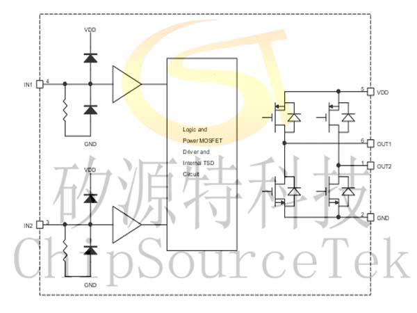
The circuit adopts H-bridge structure and built-in power MOSFET switch, which can control the forward rotation, reverse, braking and standby of the load DC motor. The braking function can make the load motor stop rotating quickly, and the standby function makes the static power consumption of the circuit very low (less than 1uA).
The circuit has a built-in low-resistance power MOSFET switch. Under the condition of 300mA load current, the circuit generates a voltage drop of 500mV and a power consumption of 150mW. Within the range allowed by the SOT23-6 package, the circuit can work continuously for a long time.
The FM116C has built-in thermal protection (TSD) with hysteresis effect. The maximum continuous output current of FM116C is 600mA at 27℃ and VDD=4V. Affected by the heat dissipation capacity of the package As the ambient temperature increases, the maximum continuous output current must be appropriately reduced.
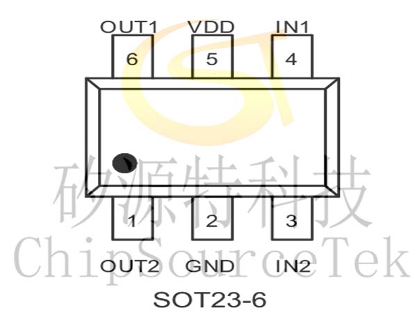
FM116C is available in SOT23-6 package.
FM116C Features:
Single channel H-bridge driver with built-in PMOS/NMOS power switch
There are four functions: forward/reverse/stop/brake
Low standby current (typ.0.1uA)
Wide operating voltage range, suitable for lithium battery supply (2.5V~5V)
500mA current output capacity (VDD=4V,RL=5Ω)
FM116C Built-in Thermal Protection with Hysteresis (TSD)
CMOS input, input without additional current limiting resistance
The FM116C is available in a SOT23-6 package
FM116C Product Application:
Toy DC motor drive
Remote-controlled toy aircraft tail motor drive
Remote control toy aircraft steering motor drive
FM116C Typical application circuit diagram:

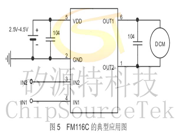
 | Serial number | Pin name | Input/output | Pin specification |
1 | OUT2 | O | Reverse the drive output | |
2 | GND | -- | Ground terminal | |
3 | IN2 | I | Invert the control signal input | |
4 | IN1 | I | Forward turn control signal input | |
5 | VDD | O | Power terminal | |
6 | OUT1 | O | Forward drive output |

IN1 | IN2 | OUT1 | OUT2 | Feature |
L | L | Z | Z | Standby (stop) |
H | L | H | L | forword |
L | H | L | H | reversal |
H | H | L | L | brake |
argument | symbol | value | unit |
Supply voltage | VDDMAX | 6.5 | V |
Maximum applied output voltage | VOUTMAX | VDD | V |
Maximum external input voltage | VINMAX | VDD | V |
Peak output current | IOUTMAX | 0.8 | A |
Maximum continuous output current | IOUTC | 0.60 | A |
Maximum power consumption | 0.6 | W | |
Junction temperature to ambient thermal resistance | θJA | 220 | ℃/W |
Operating temperature range | Topr | -20~+85 | ℃ |
Junction temperature | TJ | 150 | ℃ |
Storage temperature | Tstg | -55~150 |

Please submit your basic information, send an email to Sales@ChipSourceTek.com, or call us at 13823761625 (same number as WeChat), and we will contact you as soon as possible!

WeChat Official Account

WeChat Service
 Email
Email QQ
QQ 13823761625
