
Products
Products
FM9689
FM9689 is a lithium battery charging and discharging power management IC that integrates lithium battery charging management, high-efficiency boost discharge output, LED light power indicator, and button function module.
The DC-DC synchronous boost module of FM9689 integrates internal power MOS transistors, providing 5V/0.5A output and up to 90% boost conversion efficiency. The output voltage can achieve an accuracy of ± 1%.
The DC-DC synchronous boost module of FM9689 integrates internal power MOS transistors, providing 5V/0.5A output and up to 90% boost conversion efficiency. The output voltage can achieve an accuracy of ± 1%.
FM9689 Description:
FM9689 is a lithium battery charging and discharging power management IC that integrates lithium battery charging management, high-efficiency boost discharge output, LED light power indicator, and button function module.
FM9689 is charged in a linear manner, integrating the entire charging process including trickle charging, constant current charging, and constant voltage charging. The floating charging voltage accuracy can reach ± 1% over the entire temperature range, and it has the advantages of small charging current ripple and stable output voltage.
The DC-DC synchronous boost module of FM9689 integrates internal power MOS transistors, providing 5V/0.5A output and up to 90% boost conversion efficiency. The output voltage can achieve an accuracy of ± 1%.
FM9689 has multiple protection designs, including load overcurrent protection, input overvoltage protection, output current limiting protection, output short circuit protection, and chip over temperature protection. At the same time, the chip port is designed with high-performance ESD protection circuits, making the chip highly reliable.
FM9689 is equipped with an automatic load recognition function, which automatically activates the boost output when a load is detected;
FM9689 currently offers the packaging form of SOP8.
FM9689 currently offers the packaging form of SOP8.
FM9689 Features:
The peripheral circuit is simple and does not require an external MOS
Programmable charging current, maximum 0.3A@5V
Low standby current, FM9689 standby current is about 6uA
Full charge voltage optional, floating charge voltage accuracy ± 1%
Programmable charging current, maximum 0.3A@5V
Low standby current, FM9689 standby current is about 6uA
Full charge voltage optional, floating charge voltage accuracy ± 1%
Soft start function
Trickle current/constant current/constant voltage three-stage charging
Can achieve maximum 0.5A@5V Boost output
The overall plan can achieve a maximum efficiency of 90% in boosting voltage
After the input power is turned on, the battery will automatically boost and supply power in case of power failure
Multiple protection designs such as output current limiting protection and short circuit protection
Turn off the boost function during no-load detection, and the default current value for no-load judgment is about 7mA
No load judgment current 1~7mA, adjustable in multiple levels
Can drive 2 LEDs to indicate charging and discharging status
Support charging DATA protocol
FM9689 provides SOP8 packaging
FM9689 Applications:
TWS wireless Bluetooth earphone charging case
Other portable devices
Other portable devices
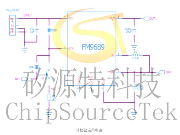
FM9689 Schematic diagram of typical application with protocol:
FM9689 Typical application schematic without protocol:

FM9689 Application Description:
1. Selection of capacitors:
CBAT, COUP, and CVIN capacitors are filtering capacitors that can use ceramic capacitors. It is recommended to choose 10V for voltage resistance, as increasing the capacitance value will make the system more stable. In any case, choosing capacitors with poor quality may cause a decrease in overall system performance, shortened service life, or even malfunction, so please choose capacitors carefully.
2. Selection of inductance L1:
It is recommended to use shielded inductors, but unshielded inductors can also be used to reduce costs. If the inductance value is 2.2uH, different inductance values will affect the no-load detection current. Please refer to the measured data for accuracy.
3. Boost load test:
Due to the addition of two-stage short-circuit protection on the chip, there are certain requirements for the boost load test:
If the USB is connected to a large capacitive load (some models of load gauges have very large capacitors), it is possible to misjudge the short-circuit protection.
When simulating a battery with a voltage source, the transient response of various types of power sources may be different, and the impedance of the power line may also be relatively high. Short circuit protection may also occur when boosting with CC or CR load or starting with load. In practical applications, the situation of CC or CR will be improved due to the connection of the battery. Generally, the input capacitance of portable devices is relatively small, and they will detect the input voltage. If the input voltage is not enough, they will not charge, so there will be no misjudgment or short circuit when charging portable devices with mobile power products.
FM9689 PCB Layout precautions:
1. High current circuit
The high current circuit refers to the devices and wiring that carry high currents during switching. In this system, it consists of L1, CBAT, COUP, and their connections. Their wiring should be as wide and short as possible. The high-frequency switch (current discontinuous) path should not pass through the through-hole, and CBAT and L1 must be on the same side of the PCB and placed together.
The high current circuit refers to the devices and wiring that carry high currents during switching. In this system, it consists of L1, CBAT, COUP, and their connections. Their wiring should be as wide and short as possible. The high-frequency switch (current discontinuous) path should not pass through the through-hole, and CBAT and L1 must be on the same side of the PCB and placed together.
2.GND
The OUT and GND pins of FM9689 are respectively the power supply and ground of the chip driving part. During the operation of the switch, there will be instantaneous large currents flowing in and out. Therefore, when drawing the PCB, the negative terminal of CBAT and GND should be as close as possible and not through holes.
3. Placement of capacitors
All capacitors must be placed close to the chip.
4. WTP wiring
Pay attention to bypassing inductor L1 when routing WTP to avoid interference.
4. WTP wiring
Pay attention to bypassing inductor L1 when routing WTP to avoid interference.
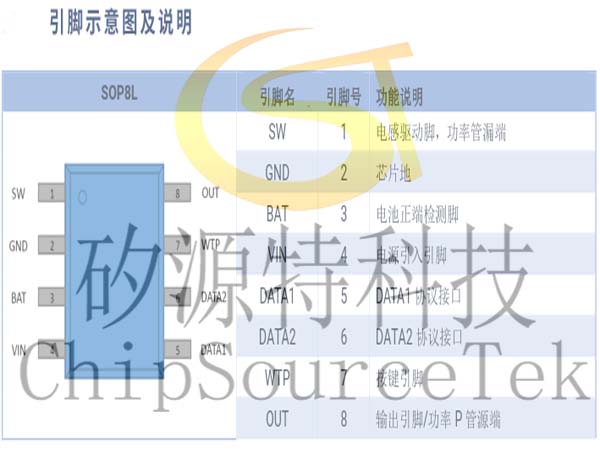
FM9689 Foot position diagram and foot position definition diagram:
FM9689 State transition diagram:


Please submit your basic information, send an email to Sales@ChipSourceTek.com, or call us at 13823761625 (same number as WeChat), and we will contact you as soon as possible!

WeChat Official Account

WeChat Service
 Email
Email QQ
QQ 13823761625
