Test method: The accurate filtering method of class D mode
In the world of audio amplifier chips, the Class D mode is favored for its energy-efficient characteristics. However, in order to ensure that the test data is accurate and close to the actual application, a key step cannot be ignored - that is, adding filters to the test process. Today, let's focus on the ChipSourceTek-CST8250 star product to deeply explore the testing mystery and design essence behind it.

ChipSourceTek-CST8250, as a leader in the audio field, is not only outstanding in performance, but also reveals the wisdom and ingenuity of engineers in every detail of its PCB design. Why add filters when testing Class D patterns? There are profound scientific principles and practical experience behind it.
When the Class D power amplifier is working, its switching frequency will produce certain high-frequency noise and harmonic distortion. If these interfering signals are directly entered into the test system without processing, the accuracy and reliability of the test results will be seriously affected. At this point, the role of the filter is particularly important. It can effectively suppress these high-frequency noise and harmonic components, making the test data more pure and accurate, so as to more accurately reflect the performance of the chip in the actual working state.

AUX-0025 is our carefully selected filter model. With its excellent filtering effect and stable performance, it has become the right-hand man in the testing process of the ChipSourceTek-CST8250. By cleverly integrating AUX-0025 filters into the test circuit, we can effectively improve the accuracy of the test data, providing a solid foundation for subsequent product development and optimization.
In the pursuit of accurate testing, we don't stop there. In order to further simulate the actual application environment and improve the practicability and reliability of the test, we also series an inductor at the RL load end. This seemingly small change actually contains great wisdom. As a common form of load, there are often parasitic inductors inside the horn, which will affect the performance of the circuit to a certain extent. Through the series inductance at the RL load end, we successfully simulated the complex factors in the practical application scenario, which made the test results more close to the reality, and provided a valuable reference for the final design of the product.

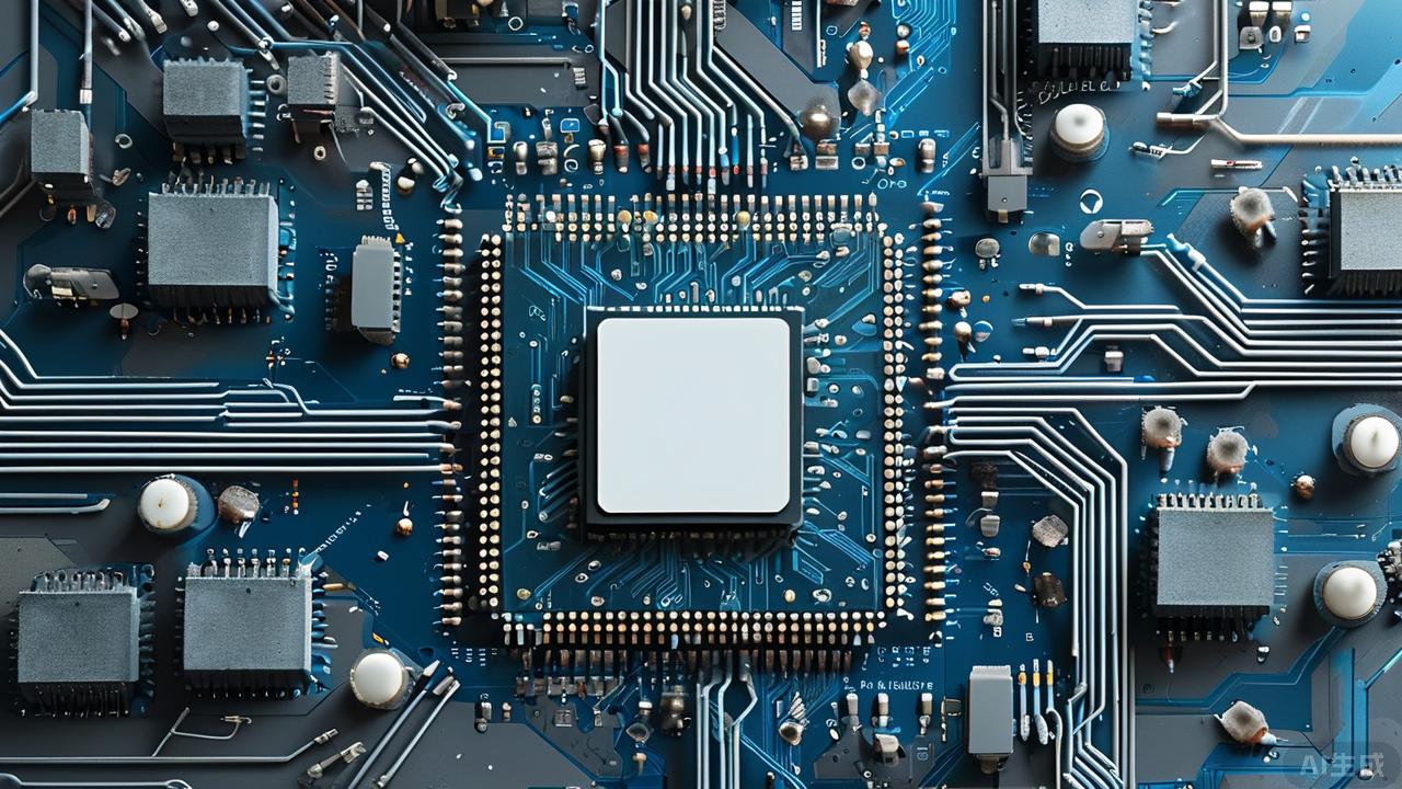
Having said the importance of the test method, let's turn our attention to the PCB design considerations of the ChipSourceTek-CST8250. An excellent product cannot be separated from a well-designed circuit board layout. For the ChipSourceTek-CST8250, proper PCB design is the key to stable operation and excellent performance.
The wiring design of power supply pins (VDD, PVDDL, PVDDR) is the first issue we must pay attention to. Since the power supply line assumes the important task of providing stable power for the entire chip, its line should be as thick as possible to reduce resistance loss and voltage drop. At the same time, when the power line must be punched through the hole, we strongly recommend the use of porous connection, and appropriately increase the hole diameter. This design can significantly reduce the resistance at the hole, ensuring the stability and reliability of the power supply. In addition, the power capacitor should also be placed as close to the pin as possible to minimize the inductance effect on the power path and improve the response speed and stability of the entire system. The key to superior performance.

Input capacitance (Cin) and input resistance (Rin) are the first threshold for signals to enter the chip, and their layout is also critical. In order to effectively suppress the noise interference caused by other signal coupling and improve the purity and accuracy of signal input, we recommend that the input capacitance and input resistance be placed as close as possible to the power amplifier chip pin. At the same time, it is also a very effective strategy to use the way of wrapping the ground. This way of routing can form a closed electromagnetic shielding layer, block the interference of external noise to signal transmission, and ensure that the audio signal maintains high fidelity characteristics during transmission.

The Bypass capacitor acts as a "cleaning agent" in the circuit, and its role cannot be underestimated. In order to give full play to the function of Bypass noise and stable voltage, it is recommended to place the bypass capacitor as close as possible to the chip pin. This can reduce the inductance effect generated by the capacitor's own leads, ensuring that it can respond quickly when needed and effectively filter out noise interference.

ChipSourceTek-CST8250 will generate a certain amount of heat accumulation during operation, if not timely heat dissipation, will affect its performance and even cause damage. To solve this problem, we recommend that the bottom heat sink of the ChipSourceTek-CST8250 be firmly welded to the PCB board. In this way, the heat generated by the chip can be effectively conducted to the PCB board and distributed through the heat dissipation path.

In order to further improve the heat dissipation effect, we also recommend that the PCB use a large area of copper to connect the heat sink in the middle of the chip. The large area of copper coating can not only increase the heat dissipation area, but also form more heat dissipation channels through the design of copper exposure, helping the chip heat dissipation more quickly. This design idea is practical and efficient, and provides a strong guarantee for the long-term stable operation of ChipSourceTek-CST8250.
ChipSourceTek-CST8250 as an audio amplifier chip, its output quality directly affects the final sound quality performance. Therefore, in PCB design, we also need to pay special attention to the pin wiring problem of its output connected to the horn. In order to reduce loss and interference during signal transmission, we require that the pin line of the output connected to the horn be as short and wide as possible. The short and wide track can reduce the resistance and inductance effects of the track, ensuring that the audio signal can be transmitted quickly and accurately to the horn end. At the same time, the cable width should be kept above 0.4mm, which can further reduce the cable impedance and voltage drop loss, and ensure the high-quality transmission of audio signals.

ChipSourceTek-CST8250 demonstrates a high degree of professionalism and rigor both in the selection of test methods and in all aspects of PCB design. These carefully designed details not only ensure the accuracy and reliability of the test data, but also lay a solid foundation for the final performance of the product. In the future project development, we believe that these valuable experience and knowledge will guide us to go further and more stable.
2. ChipSourceTek-CST8250 is a 2*8.0 audio power amplifier with dual channel AB/D class power amplifier, low distortion and low noise, supporting one line pulse control, headset and power amplifier mode switching - Sohu.com
3. ChipSourceTek-TC118AH is a single channel built-in power MOS full bridge...
4. ChipSourceTek-CST100P03 is a TO252 package,30V,100A...
5. ChipSourceTek-CST5080F is a dual series battery balanced charge management chip - Sohu


