
Well, I now need to understand the functions and applications of the ChipSourceTek-CST6307 brushed DC motor driver. First, according to the overview provided, it is a single-channel H-bridge driver suitable for a voltage range of 6.5V to 25V with a peak current of 3.6A. Internal current modulation is integrated to set the operating current through external resistors of VREF and ISEN. There is also a PWM control interface for easy connection to the controller. In addition, there is a low-power sleep mode, as well as UVLO and overheat protection. The package is e-SOP8 with heat sink.
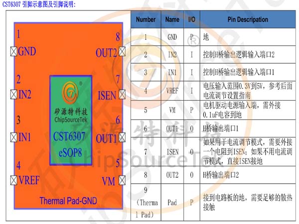
First, I need to confirm its basic structure and pin configuration. For example, the e-SOP8 package usually has eight pins, but the specific function of each pin may need to be checked in the data sheet. However, the user does not give a pin definition, so it may be necessary to assume or infer from the structure of common H-bridge drivers. For example, this might include power VM, ground GND, two control inputs IN1 and IN2, PWM inputs, VREF, ISEN, and two outputs connected to the motor OUT1 and OUT2. There may also be a SLEEP control pin, such as sleep or STBY.
Next, the current regulation function. According to the description, current regulation is based on VREF and ISEN voltage. The ISEN here should be the current detection pin, which measures the motor current through the external sensing resistance. The VREF may be used to set the reference voltage and thus determine the threshold of the current. You may need to calculate how to set the external resistance and VREF to get the desired current limit value. For example, if the voltage of the ISEN is proportional to the voltage drop of the sensing resistance, the current limit may be determined by the value of both the VREF and the sensing resistance. The specific formula may need to refer to the data book, but the user does not provide it, so it needs to be hypothesized or derived.
For example, suppose the voltage of the ISEN pin is equal to the sensing resistance Rsense multiplied by the motor current I, i.e. VISEN = I * Rsense. The VREF sets a threshold voltage, and when VISEN exceeds the VREF, the current regulating circuit acts to limit the current. Then current limit I_limit = VREF/Rsense. For example, if VREF is set to 0.5V and Rsense is 0.1 ohms, then I_limit is 5A. However, according to the specification, the peak is 3.6A, so perhaps the VREF range or Rsense selection needs to be adjusted within this range. It may be necessary to pay attention to the maximum allowable VREF value, or there may be circuits such as partial voltage inside.
Then there is PWM control. The user mentioned that the speed can be controlled through the PWM interface. In general, the H-bridge driver can control the motor speed by changing the duty cycle of the PWM to adjust the average voltage. However, the current attenuation mode is also mentioned here, which may involve the synchronous or asynchronous modulation mode of PWM, affecting the continuation path of the current. You may need to set the logic level of IN1 and IN2 to determine the direction, and then adjust the speed with the PWM signal. For example, IN1= high, IN2= low, when the PWM input is high, the motor is turning forward, and the duty cycle adjusts the speed; And vice versa. Or perhaps the PWM signal is fed directly to one of the control pins and the other pin controls the direction.
In addition, sleep mode sets the two logical inputs to low level, at which time the drive enters a low power state. So IN1 and IN2 both go to sleep when they are low, which may require care to avoid accidental sleep in the design. For example, when the motor needs to be stopped, it may be necessary to leave IN1 and IN2 in the same state, or use brake mode, rather than set low at the same time.
Regarding the protection function, UVLO is an undervoltage lock, which turns off the output when the power supply voltage falls below a certain threshold, preventing abnormal operation when the voltage is low. Overheat protection TSD will turn off the output when the chip temperature is too high, and automatic recovery may mean that the temperature is automatically restarted when the temperature drops. These protection functions need to ensure that they do not trigger frequently in the application, such as proper heat dissipation and stable power supply voltage.
Applications, suitable for high-current toys, robots, printers and so on. It is necessary to ensure that the operating voltage and current of the motor are within the specification range of Silicon Source ChipSourceTek-CST6307. For example, the rated current of the motor should not exceed the peak 3.6A, otherwise it may damage the chip. At the same time, the low on-resistance (560mΩ) can reduce the power loss, but the high current may still heat, so the need for appropriate heat dissipation, especially the e-SOP8 package although there is a heat sink, but may need PCB design heat dissipation measures, such as sufficient copper area.
When designing a circuit, the following steps may be required:
1. Determine the range of the power VM, ensure that it is between 6.5V and 25V, and consider the operating voltage of the motor.
2. Connect the control signals IN1, IN2 and PWM, which may require logic levels to match the controller, such as 3.3V or 5V.
3. Set the peripheral circuits of VREF and ISEN and select the appropriate Rsense to set the current limit. For example, if a maximum current 3A is required, VREF might be set to 0.36V (if the formula is I_limit = VREF/Rsense), then Rsense = 0.36V / 3A = 0.12Ω. However, you need to verify that the VREF scope allows such a value.
4. Connect the motor to OUT1 and OUT2.
5. Add the necessary filter capacitors, especially near the VM pins, although the description mentions that large-capacity capacitors are not required, but still need to be properly decoupled.
6. Deal with heat dissipation, heat dissipation through the copper layer of the PCB, or additional heat sink.
7. Save power by setting IN1 and IN2 to sleep when no drive is needed.
8. Handling possible fault situations, such as UVLO and TSD, may require monitoring or indicating circuits.
Possible questions:
-Source of VREF: Externally supplied voltage, or internally generated? If it is external, you may need to use a DAC or a divider resistor to set it up.
- How the ISEN is connected: Is it connected directly to one end of the sensing resistor, with the other end grounded or otherwise?
- How does current regulation work: Limit peak current or average current? Does it affect the effectiveness of PWM control?
- PWM frequency range: Is there a recommended frequency, such as avoiding too high to cause switching loss, or too low to cause motor noise?
- How to implement the current decay mode and do I need to configure specific control logic?
For example, suppose the ISEN pin is connected to the low end of the sensing resistance and the other end of the resistance is grounded. As the current flows through the motor and the sensing resistance, the voltage of the ISEN rises, compared to the VREF, and if it exceeds, the driver limits the current. In this way, the Rsense selection needs to be small enough to reduce power consumption, but large enough to produce a detectable voltage. For example, if the maximum current is 3.6A and Rsense is 0.1Ω, then the voltage drop is 0.36V, and perhaps the VREF needs to be set to 0.36V. However, you need to make sure that the input range of the VREF allows this value, such as whether the maximum VREF is a certain value, such as 0.5V or higher.
In addition, PWM control may be directed by IN1 and IN2 inputs, such as a combination of IN1 and IN2, while the PWM signal is input to one pin and the other remains at a fixed level. Alternatively, there may be a dedicated PWM input pin, but depending on the description, it may be that the PWM is input via IN1 or IN2. For example, IN1 is set to high, IN2 inputs the PWM signal, which is switched on when the PWM is high and off when it is low, and the speed is adjusted by changing the duty cycle.
It is also possible that the driver internally supports different attenuation modes, such as fast or slow attenuation, which can affect the current ripple and efficiency of the motor. However, it is not specified in the information provided by the user, and it may be necessary to assume that it is a fixed mode, or to select by controlling the input.
In terms of PCB layout, large current paths (such as VM, OUT1, OUT2, GND) require sufficient line width, reducing resistance and inductance. Sensing resistor Rsense should be as close to ISEN and GND as possible to reduce noise interference and improve the accuracy of current detection. VREF wiring should also be careful to avoid noise and may require bypass capacitors.
When testing, you need to verify whether the current limit is effective, you can measure the current when the motor is blocked to see whether it is limited to the set value. At the same time, it is necessary to test whether the PWM control smoothly adjusts the speed, and whether the power consumption of the sleep mode meets the expectations.
Possible problems:
- Inaccurate current limits: may be due to the accuracy of Rsense or voltage instability of VREF.
- Overheating: Long periods of high load may cause TSD to trigger, and heat dissipation needs to be optimized.
- Noise interference: PWM signal or current detection may be interfered with, affecting performance.
- Logic level incompatibility: Whether the output level of the controller matches the input requirements of the CST6307, such as whether level switching is required.
In summary, the design should focus on the power supply, control signal, current limit setting, heat dissipation and protection functions.
ChipSourceTek-CST6307 is a high performance brushed DC motor driver for a variety of high current applications. The following is a systematic summary of its functions, design considerations, and applications:
- ChipSourceTek-CST6307 Key features and functions
- Driving ability
- Voltage range:6.5V–25V,Suitable for medium and high voltage motor.
- Peak current:3.6A,Meet high current requirements (e.g., starting/stopping).
- Low on-resistance:The total internal resistance of the H bridge is 560mΩ (HS+LS), which reduces the power loss.
- Control interface:
- PWM speed regulation:Motor speed is adjusted by duty cycle to support current attenuation mode to optimize efficiency.
- Logical input:The IN1/IN2 controls steering (forward/reverse/brake), and the dual low power level enters sleep mode (<1µA).
- Current regulation:
- Simulation Settings:The current limit is set by the VREF pin voltage and the external sensing resistance (Rsense), the formula is:
- �limit=�REF�sense
- Ilimit
- =Rsense
- VREF
- ISEN pin:Monitor Rsense voltage drop and dynamically limit current to reduce system power consumption and capacitance requirements.
- Protection mechanism:
- UVLO:Undervoltage lock (Turns off output when VM < threshold).
- TSD:Overheat shutdown (automatic recovery after the junction temperature exceeds the limit).
- Automatic fault recovery:The system automatically restarts after the exception is cleared.
- Package:The e-SOP8 has a heat sink, which needs to be designed with PCB copper layer heat dissipation.
ChipSourceTek-CST6307 Design steps and precautions
- Power supply and motor configuration:
- VM pin:Ensure that the input voltage is 6.5-25V, and place a low ESR capacitor nearby (e.g. 10µF ceramic +100nF decoupling).
- Motor selection:The rated current is lower than the peak 3.6A to avoid continuous over-limit triggering of TSD.
- Current limit Settings:
- Rsense selection:Calculated according to the target I_limit and VREF, for example:
- If VREF=0.5V, I_limit=3A → Rsense=0.5V/3A≈0.167Ω (power ≥0.5W).
- VREF generation:Can be output via divider resistor, DAC or LDO, need stable low noise.
- Control signal connection:
- IN1/IN2 logic:Match controller level (3.3V/5V), recommended truth table:
- IN1IN2 Motor state HL forward (PWM speed regulation) LH reverse (PWM speed regulation) LL Sleep mode HH brake (low resistance)
- PWM frequency:10-20khz (balance noise and efficiency) is recommended to avoid excessive switching loss.
- PCB layout optimization:
- High current path:Thicker VM, OUT1/OUT2, GND cables to reduce pressure drop and thermal stress.
- Sensitive signal:ISEN and VREF are far away from high frequency noise sources, and Rsense uses Kelvin connection.
- Heat dissipation design:Connect the chip heat sink with copper and add through hole heat dissipation if necessary.
- Protection and Testing:
- TSD Monitoring:It can be verified by temperature rise experiment to ensure that the heat dissipation meets the continuous working requirements.
- Current verification:Locked-rotor motor to measure whether the current is stable at the set I_limit.
- Sleep mode:Static current test, confirm IN1/IN2 low power consumption <1µA.
ChipSourceTek-CST6307 Typical application scenario
- Robot joint drive:PWM is used to accurately control the speed, and current limit protects the motor from rotation.
- POS machine print head:Fast start-stop response, low on-resistance reduces heat.
- Electric toy car:Supports high burst current (3.6A peak) for complex loads.
- Home appliance valve control:Hibernation mode reduces standby power consumption and is suitable for battery-powered scenarios.
ChipSourceTek-CST6307 Common Problems and solutions
- Large current fluctuation:Check Rsense layout and VREF stability, increase filter capacitance.
- Frequent triggering of TSD:Optimize heat dissipation (such as increasing copper area or forcing air cooling) to reduce ambient temperature.
- Motor jitter:Adjust PWM frequency to avoid resonance points; Check IN1/IN2 signal timing.
With proper configuration of peripheral circuits and PCB design, ChipSourceTek-CST6307 can efficiently drive a wide range of brushed DC motors with both performance and reliability, making it ideal for high-current compact applications.


WeChat Official Account

WeChat Service
 Email
Email QQ
QQ 13823761625
