
Products

LTK52201
LTK52201 can output at least 2x25W or more in BTL mode and at least 45W or more in PBTL mode without the need for a heat sink.
LTK52201 is a Class D audio power amplifier designed to drive bridge stereo BTL or mono PBTL, with high efficiency and no filters.
LTK52201 can output at least 2x25W or more in BTL mode and at least 45W or more in PBTL mode without the need for a heat sink.
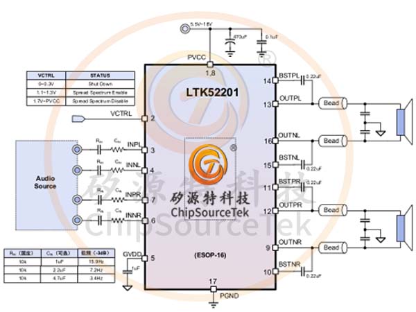
Advanced spread spectrum function and advanced electromagnetic interference (EMI) suppression technology can meet electromagnetic compatibility (EMC) requirements while allowing users to choose not to use or use low-cost magnetic bead filters at the output end according to their needs.
LTK52201 has a bottom noise as low as 60uV, excellent on/off burst suppression function, and ultra-low THD+N distortion across the entire frequency range.
The DC detection function can measure the frequency and amplitude of pulse width modulation (PWM). If the input capacitor is damaged or the input terminal is short circuited, LTK52201 will shut down the output stage, which can effectively protect various speakers.
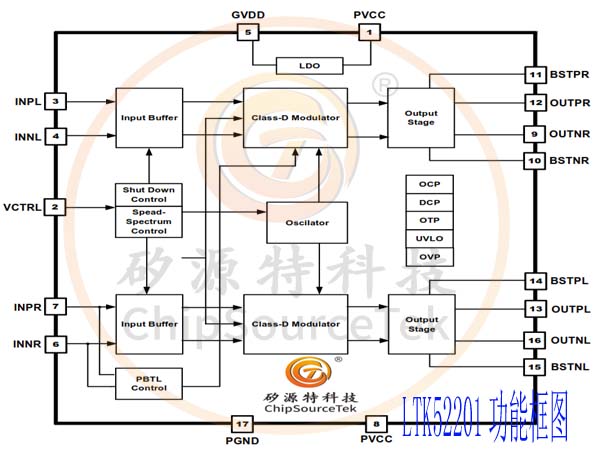
LTK52201 has various comprehensive circuit protection mechanisms, including automatic recovery function for ground, power, mutual short circuit protection, thermal protection, undervoltage and overvoltage protection.
LTK52201 Feature:
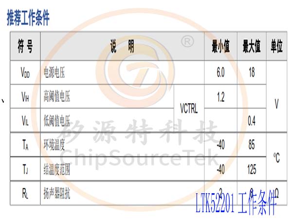
Working voltage range: 6.0V -18V
PBTL mode applicable to mono
Fixed 26dB gain
output power
BTL Mode:
at 10% THD+N
– 2x18.3W, at VDD =12V, RL =4Ω
– 2x28.0W, at VDD =15V, RL =4Ω
– 2x29.0W, at VDD =18V, RL =6Ω
at 1% THD+N
– 2x15.2W, at VDD =12V, RL =4Ω
– 2x23.0W, at VDD =15V, RL =4Ω
– 2x23.5W, at VDD =18V, RL =6Ω
PBTL Mode :
at 10% THD+N
– 35.5W, at V DD =12V, R L =2Ω
– 40.0W, at V DD =15V, R L =3Ω
– 45.0W, at V DD =18V, R L =4Ω
DC detection protection function for protecting speakers
Efficiency of up to 90% in Class D operations reduces the requirement for heat sinks
Ultra low noise floor: 76uV (26dB, A-Weighting)
Filter free, low EMI design with spread spectrum capability
A comprehensive protection mechanism, including short-circuit protection with automatic recovery function, thermal protection, DC detection, and undervoltage and overvoltage protection, etc
Excellent THD+N and no popping sound design
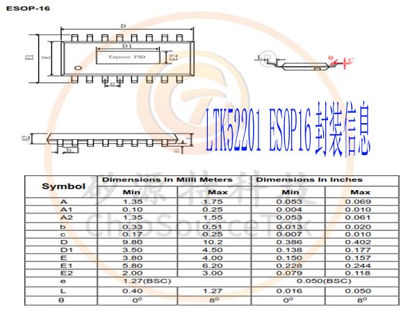
Environmentally friendly packaging ESOP-16 that meets ROHS requirements
LTK52201 Application:
Various Bluetooth speakers, smart speakers
Television and monitor
Various home entertainment devices
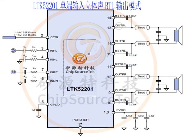
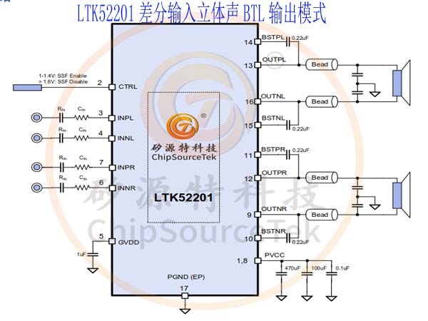
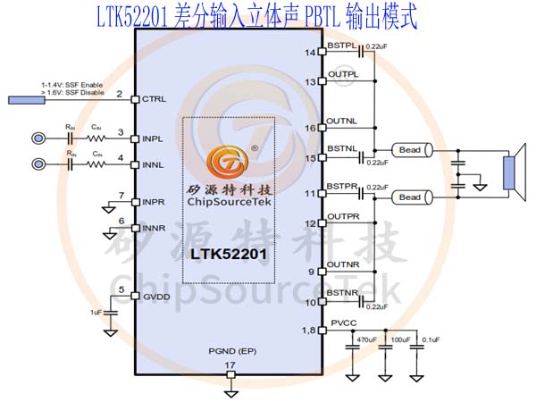
LTK52201 Typical Application Circuit:

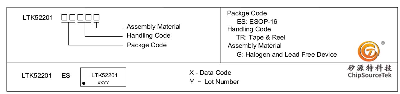
LTK52201 Encapsulate ordering information:
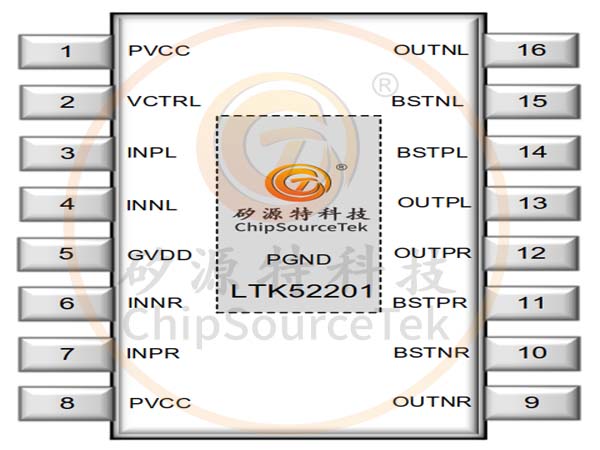
LTK52201 Pin description:

LTK52201 Pin description:

LTK52201 Functional Block Diagram:

LTK52201 Recommended working conditions:

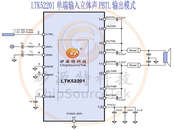
LTK52201 Typical Application Circuit:


LTK52201 Application Guide:
LTK52201 is an ultra-low noise, high-efficiency stereo D-class audio power amplifier that can operate in the range of 6.0V to 18V. With a 15V 4 Ω speaker, it can provide 2x23W output power (THD+N=1%) and 2x28W output power (THD+N=10%).
The LTK52201 has an efficiency of up to 90%, which can extend the working time of the power battery. On a double-layer circuit board, it provides at least 2x25W of output power without the need for an additional heat sink.
The advanced spread spectrum function can further reduce EMI radiation and even meet requirements without adding any magnetic beads.
LTK52201 drives dual speakers in BTL mode or uses parallel output, while in PBTL mode, it provides double output capability through mono output. At the same time, LTK52201 has comprehensive protection functions, including various short-circuit protection, over temperature protection, under voltage and over voltage protection, and so on.
In order to prevent DC bias damage to the speaker in the event of input capacitor damage or accidental grounding, LTK52201 integrates DC detection protection function.
LTK52201 PCB Application Guide:
When designing the PCB for LTK52201, attention should be paid to high current routing, and the connections between the power supply and the chip input PVCC, as well as between (OUTPL/R and OUTNL/R) and the speaker, should be as thick and short as possible to reduce parasitic resistance losses.
The heat sink under the chip must be directly and reliably soldered to the solder pads of the PCB, including the front and back sides, leaving a large and uninterrupted grounding area as much as possible (i.e. no wires passing through the grounding layer to obstruct the heat flow near the chip), and placing a large number of solid metal through holes between the front and back sides to connect the grounded top and bottom layers. All power ground pins PGND are directly short circuited to the ground plane ground to reduce the coupling of high current switch noise to audio signals.
In order to reduce the bottom noise of the system, differential input mode should be used as much as possible, and the input resistors and capacitors of INNL, INPL, INNR, and INPR should be matched as much as possible; When using single ended input, one end of the input is AC grounded, and the wire needs to be pulled to the signal source end and then grounded to make the input paths of INNL, INPL, INNR, and INPR as symmetrical as possible.
Suitable decoupling capacitors should be placed at the power input PVCC, and the capacitors should be placed as close as possible to the corresponding power pins and ground.
To further reduce EMI, series magnetic beads can be added to the output of the power amplifier and a capacitor can be connected to ground to better suppress high-frequency EMI.
The output power of LTK52201 is relatively high. If the heat dissipation measures are not done well, it will affect normal operation. In order to ensure that the chip works normally and reliably at maximum output power,
There are the following guiding principles for optimal heat dissipation performance:
Fill large solid grounding metal layers on the upper and lower layers of the PCB board to help dissipate heat.
Weld the heat dissipation pads of the chip directly and reliably onto the grounded metal plane.
Reserve a wide and uninterrupted metal area around the bottom of the chip, where no wires pass through the ground layer and block heat flow.
Place many solid through holes with the same spacing under the heat dissipation pads of the chip where the upper and lower grounding layers are connected.
Try to avoid using through holes for high current connections (such as power supply to PVCC, output to speaker connections).
LTK52201 Encapsulation information:


Please submit your basic information, send an email to Sales@ChipSourceTek.com, or call us at 13823761625 (same number as WeChat), and we will contact you as soon as possible!

WeChat Official Account

WeChat Service
 Email
Email QQ
QQ 13823761625
