
Products
Products

PAM8403
PAM8403 is a Class D audio power amplifier IC with an output power of 3W;
PAM8403 provides up to 3W output power under 4 Ω load and 5V power supply conditions;
PAM8403 adopts lead-free SOP16 packaging.
PAM8403 provides up to 3W output power under 4 Ω load and 5V power supply conditions;
PAM8403 adopts lead-free SOP16 packaging.
PAM8403 Summary:
PAM8403 is a Class D audio power amplifier IC with an output power of 3W,
PAM8403 has the characteristics of low harmonic distortion and low noise crosstalk, which enables it to achieve good sound quality in sound playback. By adopting a new architecture with no coupling output and no low-pass filtering circuit, it can directly drive the speaker, reducing the overall cost and PCB space occupation of the solution.
Under the same number of peripheral components, the D-class amplifier IC PAM8403 has much better efficiency than the A-class amplifier, which extends the battery life and is an ideal choice for portable devices such as laptops.
PAM8403 Feature:
Class-D amplifier without filter, low static current and low EMI;
Provide up to 3W output power under 4 Ω load and 5V power supply conditions;
Up to 90% efficiency;
Low THD, low noise;
Short circuit current protection;
Thermal protection;
Very few external components, saving space and costs;
PAM8403 offers lead-free SOP16 packaging.
PAM8403 Application:
Loudspeaker box
Portable audio devices
PAM8403 Typical application circuit diagram:

PAM8403 Rated working conditions
PAM8403 is a Class D audio power amplifier IC with an output power of 3W,
PAM8403 has the characteristics of low harmonic distortion and low noise crosstalk, which enables it to achieve good sound quality in sound playback. By adopting a new architecture with no coupling output and no low-pass filtering circuit, it can directly drive the speaker, reducing the overall cost and PCB space occupation of the solution.
Under the same number of peripheral components, the D-class amplifier IC PAM8403 has much better efficiency than the A-class amplifier, which extends the battery life and is an ideal choice for portable devices such as laptops.
PAM8403 Feature:
Class-D amplifier without filter, low static current and low EMI;
Provide up to 3W output power under 4 Ω load and 5V power supply conditions;
Up to 90% efficiency;
Low THD, low noise;
Short circuit current protection;
Thermal protection;
Very few external components, saving space and costs;
PAM8403 offers lead-free SOP16 packaging.
PAM8403 Application:
Loudspeaker box
Portable audio devices
PAM8403 Typical application circuit diagram:
PAM8403 Foot Map:
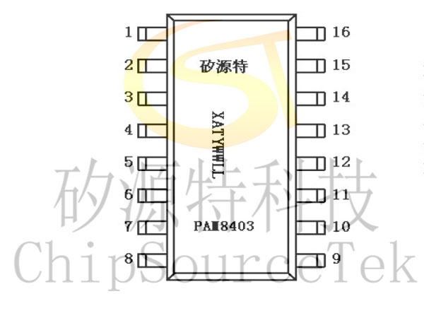
PAM8403 Pin Definition:
PAM8403 Absolute rated value(Note: This is only the maximum limit and does not guarantee operational functionality. Long term operation under extreme conditions may affect device reliability.)
PAM8403 Pin Definition:
| Serial number | Pin name | Function Description |
| 1 | +OUT_L | Left channel reverse output |
| 2 | PGND | Negative pole of power supply (left channel) |
| 3 | -OUT_L | Left channel output in the same direction |
| 4 | PVDD | Positive pole of power supply (left channel) |
| 5 | /MUTE | Mute control input (low level effective) |
| 6 | VDD | Simulate VDD |
| 7 | INT | Left channel input |
| 8 | VREF | Internal simulation reference source, connect a bypass capacitor from VREF to GND |
| 9 | NC | Hanging in the air |
| 10 | INR | Right line |
| 11 | GND | Simulated grounding |
| 12 | /SHDN | System shutdown control (low level effective) |
| 13 | PVDD | Power VDD (left channel) |
| 14 | -OUT_R | Right channel output in the same direction |
| 15 | PGND | Power Ground (Left Channel) |
| 16 | +OUT_R | Reverse output of right channel |
PAM8403 Absolute rated value(Note: This is only the maximum limit and does not guarantee operational functionality. Long term operation under extreme conditions may affect device reliability.)
Supply voltage ……………………..…………...........6.0V
Input voltage ....………………….….-0.3V to VDD+0.3V
Working temperature ……………………………..-40℃ to 85℃
Maximum junction temperature ……………………………………...150℃
Work completion temperature…………………….………..…-40℃ to 125℃
Storage temperature ………………….……………. -65℃ to 150℃
Welding temperature …………………………………… 300℃, 5sec
Input voltage ....………………….….-0.3V to VDD+0.3V
Working temperature ……………………………..-40℃ to 85℃
Maximum junction temperature ……………………………………...150℃
Work completion temperature…………………….………..…-40℃ to 125℃
Storage temperature ………………….……………. -65℃ to 150℃
Welding temperature …………………………………… 300℃, 5sec
PAM8403 Rated working conditions
Power supply voltage range ……………….………..2.5V to 5.5V
Working temperature range ………………….….. -40℃ to 85℃
Range of junction temperature ……………………………….. -40℃ to 125℃
Working temperature range ………………….….. -40℃ to 85℃
Range of junction temperature ……………………………….. -40℃ to 125℃
PAM8403 Hot information
PAM8403 Electrical characteristics (VDD=5V, Gain=24dB, RL=8Ω, TA=25℃, Unless otherwise specified。)
| Parameter | Symbol | Package | Maximum value | Company |
| Thermal resistance | θJA | DIP -16 | 90 | ℃/W |
| SOP -16 | 110 | ℃/W |
PAM8403 Electrical characteristics (VDD=5V, Gain=24dB, RL=8Ω, TA=25℃, Unless otherwise specified。)
| Symbol | Parameter | Test conditions | Minimum | Typical | Maximum | Company | |
| VIN | Supply voltage | 2.5 | -- | 5.5 | V | ||
| PD | Output power | THD+N=10%, f=1KHz, RL=4Ω | VDD=5.0V | -- | 3.2 | -- | W |
| VDD=3.6V | -- | 1.6 | -- | ||||
| VDD=3.0V | -- | 1.3 | -- | ||||
| THD+N=1%, f=1KHz, RL=4Ω | VDD=5.0V | -- | 2.5 | -- | |||
| VDD=3.6V | -- | 1.3 | -- | ||||
| VDD=3.0V | -- | 0.85 | -- | ||||
| THD+N=10%, f=1KHz, RL=8Ω | VDD=5.0V | -- | 1.8 | -- | |||
| VDD=3.6V | -- | 0.9 | -- | ||||
| VDD=3.0V | -- | 0.6 | -- | ||||
| THD+N=1%, f=1KHz, RL=8Ω | VDD=5.0V | -- | 1.4 | -- | |||
| VDD=3.6V | -- | 0.72 | -- | ||||
| VDD=3.0V | -- | 0.45 | -- | ||||
| THD+N | Total harmonic distortion+noise | VDD=5.0V, PO=0.5W, RL=8Ω | f=1KHz | -- | 0.15 | -- | % |
| VDD=3.6V, PO=0.5W, RL=8Ω | -- | 0.11 | -- | ||||
| VDD=5.0V, PO=1W, RL=4Ω | f=1KHz | -- | 0.15 | -- | |||
| VDD=3.6V, PO=1W, RL=4Ω | -- | 0.11 | -- | ||||
| GV | Gain | -- | 24 | -- | dB | ||
| PSRR | Power ripple suppression ratio | VDD=5.0V, Inputs ac-grounded with CIN=0.47uF | -- | -59 | -- | dB | |
| f=1KHz | -- | -58 | -- | ||||
| CS | Channel isolation degree | VDD=5V, PO=0.5W, RL=8Ω, GV=20dB | f=1KHz | -- | -95 | -- | dB |
| SNR | Signal-to-noise ratio | VDD=5V, Vorms=1V, GV=20dB | f=1KHz | -- | 80 | -- | dB |
| Vn | Output noise | VDD=5.0V, Inputs ac-grounded with CIN=0.47uF | A-weighting | -- | 100 | -- | uV |
| No A-weighting | -- | 150 | -- | ||||
| Dyn | Dynamic range | VDD=5.0V, THD=1% | f=1KHz | -- | 90 | -- | dB |
| η | Efficiency | RL=8Ω, THD=10% | f=1KHz | -- | 87 | -- | % |
| RL=4Ω, THD=10% | -- | 83 | -- | ||||
| IQ | Static current | VDD=5.0V | No load | -- | 16 | -- | mA |
| VDD=3.6V | -- | 10 | -- | ||||
| VDD=3.0V | -- | 8 | -- | ||||
| IMUTE | Shielding current | VDD=5.0V | VMUTE=0.3V | -- | 3.5 | -- | mA |
| ISD | Turn off the current | VDD=2.5V to 5.5V | Vsd=0.3V | -- | <1 | -- | uA |
| Rdson | On resistance | IDS=500mA, Vgs=5V | PMOS | -- | 180 | -- | mΩ |
| PMOS | -- | 140 | -- | ||||
| fsw | Conversion frequency | VDD=3V to 5V | -- | -- | 260 | -- | KHz |
| Vos | Output offset voltage | Vin=0V, VDD=5V | -- | -- | 10 | -- | mV |
| VIH | Enable Input high voltage | VDD=5.0V | -- | 1.5 | 1.4 | -- | V |
| VIL | Enable Input low voltage | VDD=5.0V | -- | -- | 0.7 | 0.4 | |
| VIH | MUTE Input high voltage | VDD=5.0V | -- | 1.5 | 1.4 | -- | V |
| VIL | MUTE Input low voltage | VDD=5.0V | -- | -- | 0.7 | 0.4 | |
| OTP | Over temperature protection | No load, junction temperature | VDD=5.0V | -- | 1400 | -- | ℃ |

Please submit your basic information, send an email to Sales@ChipSourceTek.com, or call us at 13823761625 (same number as WeChat), and we will contact you as soon as possible!

WeChat Official Account

WeChat Service
 Email
Email QQ
QQ 13823761625
