
Products
Products

8002B
The 8002B is an audio power amplifier IC with turn-off mode. On 5V power supply, the average power on the load (3Ω) is 3W, and the distortion does not exceed 10%. No output coupling capacitors or external buffer circuits are required. Stable gain output. External gain Settings.
The 8002/8002B is available in a SOP8 package.
The 8002/8002B is available in a SOP8 package.
8002/8002B概 Description
The 8002/8002B is an audio power amplifier IC with turn-off mode.
When operating at 5V input voltage, the average power on the load (3Ω) is 3W, and the distortion does not exceed 10%. For portable devices, when VDD is applied to the turn-off end,
The 8002/8002B will enter the off mode, which is extremely low power consumption, with an IQ of only 0.6uA.
The 8002/8002B is an audio amplifier IC designed for high-power, high-fidelity applications. Few peripheral components are required and can work at input voltages from 2.0V to 5.5V.
8002/8002B Features:
No output coupling capacitors or external buffer circuits are required.
Stable gain output.
External gain Settings.
Package form: SOP8, SOP8-PP, DIP8, MSOP8.
The 8002/8002B is available in a SOP8 package.
8002/8002B application
Can be applied to portable devices
Desktop computers and audio equipment for low voltage operation.
8002/8002B Typical application circuit diagram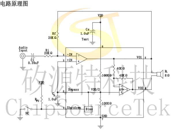
8002B Pin arrangement and description: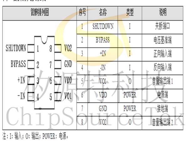
Serial number
| Serial number | name | type | Instructions |
| 1 | SHUTDOWN | I | Turn-off port |
| 2 | BYPASS | I | Voltage reference terminal |
| 3 | +IN | I | Forward input |
| 4 | -IN | I | Reverse input |
| 5 | VO1 | O | Volume output 1 |
| 6 | VDD | POWER | Power terminal |
| 7 | GND | POWER | Ground terminal |
| 8 | VO2 | O | Volume output 2 |
Note: I: input; O: Output; -Leonard: The POWER supply。
8002B Bridge Configuration
There are two operational amps in the 8002B, but their Settings are different.
The first op amp gain can be set externally with two resistors RF and RJ (+IN and -IN ports), while the second op amp gain is fixed. The output signal of the first op amp is actually the input signal of the second op amp, and the two op amps produce the same number of signals, and the phase is opposite. Therefore, the 8002/8002B gain is as follows: AVD = 2 x (Rf/Ri) is the drive load, and the op amp is set to bridge mode. The bridge mode is different from some common op-amp circuits that connect one side of the load to the ground, and can make the load produce 4 times the output power under the same conditions.
8002B Power consumption
The power consumption generated on the load is also relatively large, so under the condition of specified voltage, the load power consumption is as follows: PDMAX = 4× (VDD)2/ (2π2) RL
So input 8 at 5V? Under load, the maximum output power consumption is 625mW. But the result of this algorithm is as follows: PDMAX = (TJMAX-TA)/ θJA
Note: SOP package θJA=140°C/W, DIP package θJA=107°C/W, MSOP package θJA=210°C/W
8002B Reference voltage
The external capacitor at the voltage reference should be as close to 8002/8002B as possible. A capacitor of 0.1μF improves the stability of the internal bias voltage and reduces the effect of PSRR. You can increase the ground capacitance of the BYPASS end to improve the PSRR. The CB value depends on the requirements for the PSRR.
8002B Switch off function
To reduce power consumption, the 8002/8002B switch off the external bias circuit. When the shutdown end is high power, the op amp is turned off, and the 8002/8002B does not work, then the operating current of 8002/8002B is reduced to 0.6uA. When the turn-off terminal voltage is slightly lower than VDD, 8002/8002B is not stable. Therefore, the turn-off end should be placed at a stable voltage value to avoid the IC entering the wrong working state.
In many applications, the level conversion at the off end is done by the processor. When the one-way knife switch is used to achieve the level conversion, the pull resistance can be added to the off end, so that when the switch is off, the level of the 8002/8002B off end is in a correct state due to the pull-up resistance, so as to ensure that 8002/8002B will not enter the wrong working state.
8002B Limit parameter(Ta=25℃)
| peculiarity | symbol | Radius | unit |
| Operating voltage | VDD | 6 | V |
| Input voltage | VIN | -0.3~VDD+0.3 | V |
| Operating temperature | TOPR | -65~+150 | ℃ |
| Ambient temperature | TA | -40~+85 | ℃ |
| Node temperature | TJ | 150 | ℃ |
8002B Electrical specifications(VDD=5V,RL=8Ω,Ta=25℃)
| name | symbol | Minimum value | Typical value | Maximum value | unit | Test condition |
| Operating voltage | VDD | 2.0 | -- | 5.5 | V | |
| Static current | IDD | -- | 6.5 | 10 | mA | VIN=0V, IO=0mA |
| Turn-off current | ISD | -- | 0.6 | 2 | uA | VPIN1=VDD |
| Output bias | VOS | -- | 5.0 | 50 | mV | VIN=0V |
| Output power | PO | -- | 1.2 | -- | W | THD=1%, f=1KHz, RL=8Ω |
| -- | 1.5 | -- | THD=10%, f=1KHz, RL=8Ω | |||
| Total harmonic distortion + noise | THD+N | -- | 0.25 | -- | % | 20Hz≤f≤20KHz, AVD=2, RL=8Ω, PO=1W |
| Power supply rejection ratio | -- | 60 | -- | dB | VDD=4.9V~5.1V |
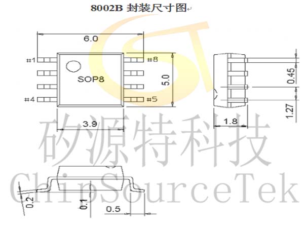
8002B package diagram:

Please submit your basic information, send an email to Sales@ChipSourceTek.com, or call us at 13823761625 (same number as WeChat), and we will contact you as soon as possible!

WeChat Official Account

WeChat Service
 Email
Email QQ
QQ 13823761625
